3312 - 2 mm SMD Trimming Potentiometer
TBU
®
High-Speed Protectors have a 100 % matte-tin termination
nish. For improved thermal dissipation, the recommended layout
uses PCB copper areas which extend beyond the exposed solder
pad. The exposed solder pads should be dened by a solder mask
which matches the pad layout of the TBU
®
device in size and spac-
ing. It is recommended that they should be the same dimension as
the TBU
®
pads but if smaller solder pads are used, they should be
centered on the TBU
®
package terminal pads and not more than
0.10-0.12 mm (0.004-0.005 in.) smaller in overall width or length.
Solder pad areas should not be larger than the TBU
®
pad sizes
to ensure adequate clearance is maintained. The recommended
stencil thickness is 0.10-0.12 mm (0.004-0.005 in.) with a stencil
opening size 0.025 mm (0.0010 in.) less than the solder pad
size. Extended copper areas beyond the solder pad signicantly
improve the junction to ambient thermal resistance, resulting in
operation at lower junction temperatures with a corresponding
benet of reliability. All pads should soldered to the PCB, includ-
ing pads marked as NC or NU but no electrical connection should
be made to these pads. For minimum parasitic capacitance, it is
recommended that signal, ground or power signals are not routed
beneath any pad.
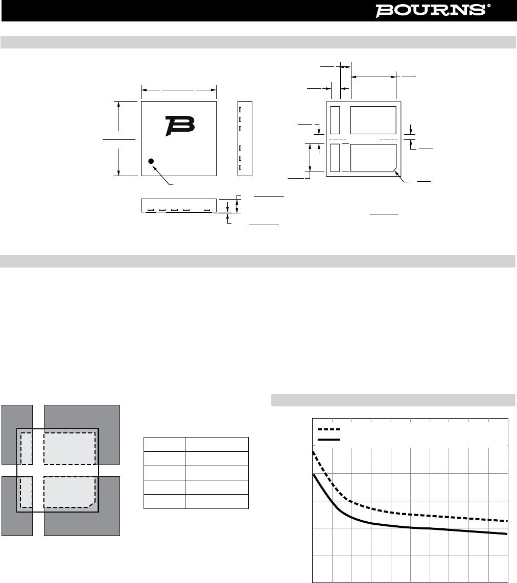
TBU-DT Series - TBU
®
High-Speed Protectors
Product Dimensions
Pad # Pin Out
1 Line Side 1
2 Line Load 1
3 Line Load 2
4 Line Side 2
Pad Designation
Recommended Pad Layout
4
1
3
2
Thermal Resistance vs. Additional PCB Cu Area
Dark grey areas show added PCB copper area for better
thermal resistance.
Added Cu Area (Sq. In.)
0 0.2 0.4 0.6 0.8 1.0 1.2 1.4 1.6 1.8 2.0
120
100
80
60
40
20
0
Thermal Resistance to Ambient (°C/W)
Typical RTH (Power in 1 TBU
®
Device)
Typical RTH (Equal Power in Both TBU
®
Devices)
Specifications are subject to change without notice.
The device characteristics and parameters in this data sheet can and do vary in different applications and actual device performance may vary over time.
Users should verify actual device performance in their specific applications.
1.85
(.073)
0.60
(.024)
0.70
(.028)
0.35
(.014)
3.05
(.120)
0.75
(.030)
C PIN 1
SYMMETRY
0.25
(.010)
PIN 1 & BACKSIDE CHAMFER
A1 =
5.00 ± 0.10
(.197 ± .004)
0.00 - 0.05
(.000 - .002)
5.00 ± 0.10
(.197 ± .004)
A =
0.80 - 1.00
(.031 - .039)
XXXXX
YWWLL
SEATING PLANE
DIMENSIONS:
MM
(INCHES)
