10
LTC1430
INTERNAL
CIRCUITRY
V
CC
/PV
CC2
LTC1430 (8-LEAD)
PV
CC1
M1
L1
M2
G1
G2
PV
CC
C
OUT
V
OUT
LTC1430 • F07
+
Figure 7. 8-Lead Power Supplies
OS-CON part number 10SA220M (220µF/10V) capacitors
feature 2.3A allowable ripple current at 85°C and 0.035
ESR; three in parallel at the input and six at the output will
meet the above requirements.
Input Supply Considerations/Charge Pump
The 16-lead LTC1430 requires four supply voltages to
operate: PV
CC
for the main power input, PV
CC1
and PV
CC2
for MOSFET gate drive and a clean, low ripple V
CC
for the
LTC1430 internal circuitry (Figure 6). In many applica-
tions, PV
CC
and PV
CC2
can be tied together and fed from
a common high power supply, provided that the supply
voltage is high enough to fully enhance the gate of external
MOSFET M2. This can be the 5V system supply if a logic
level MOSFET is used for M2. V
CC
can usually be filtered
with an RC from this same high power supply; the low
quiescent current (typically 350µA) allows the use of
relatively large filter resistors and correspondingly small
filter capacitors. 100 and 4.7µF usually provide ad-
equate filtering for V
CC
.
For both versions of the LTC1430, PV
CC1
must be higher
than PV
CC
by at least one external MOSFET V
GS(ON)
to fully
enhance the gate of M1. This higher voltage can be
provided with a separate supply (typically 12V) which
should power up after PV
CC
, or it can be generated with a
simple charge pump (Figure 4). The charge pump consists
of a 1N4148 diode from PV
CC
to PV
CC1
and a 0.1µF
capacitor from PV
CC1
to the switching node at the drain of
M2. This circuit provides 2PV
CC
– V
F
to PV
CC1
while M1 is
ON and PV
CC
– V
F
while M1 is OFF where V
F
is the ON
voltage of the 1N4148 diode. Ringing at the drain of M2
can cause transients above 2PV
CC
at PV
CC1
; if PV
CC
is
higher than 7V, a 12V zener diode should be included from
PV
CC1
to PGND to prevent transients from damaging the
circuitry at PV
CC2
or the gate of M1.
More complex charge pumps can be constructed with the
16-lead versions of the LTC1430 to provide additional
voltages for use with standard threshold MOSFETs or very
low PV
CC
voltages. A tripling charge pump (Figure 5) can
provide 2PV
CC
and 3PV
CC
voltages. These can be con-
nected to PV
CC2
and PV
CC1
respectively, allowing stan-
dard threshold MOSFETs to be used with 5V at PV
CC
or 5V
logic level threshold MOSFETs to be used with 3.3V at
PV
CC
. V
CC
can be driven from the same potential as PV
CC2
,
allowing the entire system to run from a single 3.3V
supply. Tripling charge pumps require the use of Schottky
diodes to minimize forward drop across the diodes at
start-up. The tripling charge pump circuit will tend to
rectify any ringing at the drain of M2 and can provide well
more than 3PV
CC
at PV
CC1
; all tripling (or higher multiply-
ing factor) circuits should include a 12V zener clamp diode
D
Z
to prevent overvoltage at PV
CC1
.
INTERNAL
CIRCUITRY
V
CC
LTC1430 (16-LEAD)
PV
CC2
PV
CC1
M1
L1
M2
G1
G2
PV
CC
C
OUT
V
OUT
LTC1430 • F06
+
Figure 6. 16-Lead Power Supplies
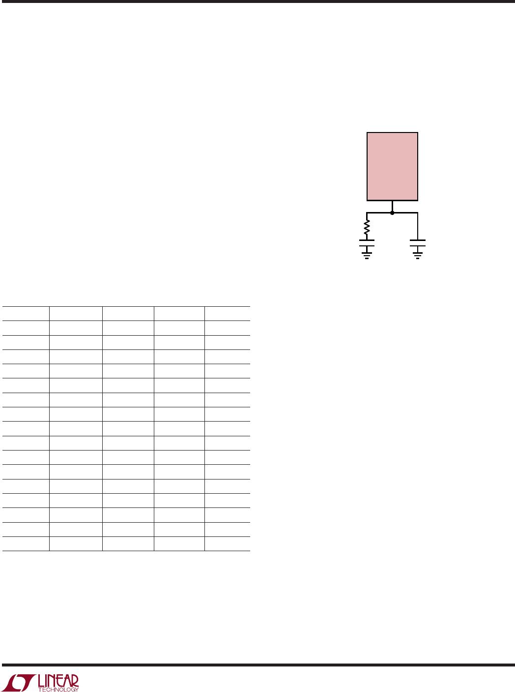
The 8-lead versions of the LTC1430 have the PV
CC2
and
V
CC
pins tied together inside the package (Figure 7). This
pin, brought out as V
CC
/PV
CC2
, has the same low ripple
requirements as the 16-lead part, but must also be able to
supply the gate drive current to M2. This can be obtained
by using a larger RC filter from the PV
CC
pin; 22 and 10µF
work well here. The 10µF capacitor must be VERY close to
the part (preferably right underneath the unit) or output
regulation may suffer.
APPLICATIO S I FOR ATIO
WUU
U
11
LTC1430
pensation components. In general, a smaller value induc-
tor will improve transient response at the expense of ripple
and inductor core saturation rating. Minimizing output
capacitor ESR will also help optimize output transient
response. See Input and Output Capacitors for more
information.
Compensation and Transient Response
The LTC1430 voltage feedback loop is compensated at the
COMP pin; this is the output node of the internal g
m
error
amplifier. The loop can generally be compensated prop-
erly with an RC network from COMP to GND and an
additional small C from COMP to GND (Figure 8). Loop
stability is affected by inductor and output capacitor
values and by other factors. Optimum loop response can
be obtained by using a network analyzer to find the loop
poles and zeros; nearly as effective and a lot easier is to
empirically tweak the R
C
values until the transient recovery
looks right with an output load step. Table 1 shows
recommended compensation components for 5V to 3.3V
applications based on the inductor and output capacitor
values. The values were calculated using multiple paral-
leled 330µF AVX TPS series surface mount tantalum
capacitors as the output capacitor.
Table 1. Recommended Compensation Network for 5V to 3.3V
Application Using Multiple 330µF AVX Output Capacitors
L1 (µH) C
OUT
(µF) R
C
(k)C
C
(µF) C1 (pF)
1 990 1.8 0.022 820
1 1980 3.6 0.01 470
1 4950 9.1 0.0047 150
1 9900 18 0.0022 82
2.7 990 3.6 0.01 470
2.7 1980 7.5 0.0047 220
2.7 4950 18 0.0022 82
2.7 9900 39 0.001 39
5.6 990 9.1 0.0047 150
5.6 1980 18 0.0022 82
5.6 4950 47 820pF 33
5.6 9900 91 470pF 15
10 990 18 0.0022 82
10 1980 39 0.001 39
10 4950 91 470pF 15
10 9900 180 220pF 10
Output transient response is set by three major factors: the
time constant of the inductor and the output capacitor, the
more impact on overall transient recovery time than the
third; unless the loop compensation is way off, more
improvement can be had by optimizing the inductor and
the output capacitor than by fiddling with the loop com-
LTC1430
COMP
GND SGND
LTC1430 • F08
C1C
C
R
C
Figure 8. Compensation Pin Hook-Up
Soft-Start and Current Limit
The 16-lead versions of the LTC1430 include a soft-start
circuit at the SS pin; this circuit is used both for initial start-
up and during current limit operation. The soft-start and
current limit circuitry is disabled in 8-lead versions. SS
requires an external capacitor to GND with the value
determined by the required soft-start time. An internal
12µA current source is included to charge the external
capacitor. Soft-start functions by clamping the maximum
voltage that the COMP pin can swing to, thereby control-
ling the duty cycle (Figure 9). The LTC1430 will begin to
operate at low duty cycle as the SS pin rises to about 2V
below V
CC
. As SS continues to rise, the duty cycle will
increase until the error amplifier takes over and begins to
regulate the output. When SS reaches 1V below V
CC
the
LTC1430 will be in full operation. An internal switch shorts
the SS pin to GND during shutdown.
The LTC1430 detects the output current by watching the
voltage at I
FB
while M1 is ON. The I
LIM
amplifier compares
this voltage to the voltage at I
MAX
(Figure 10). In the ON
state, M1 has a known resistance; by calculating back-
wards, the voltage generated at I
FB
by the maximum
output current in M1 can be determined. As I
FB
falls below
I
MAX
, I
LIM
will begin to sink current from the soft-start pin,
APPLICATIO S I FOR ATIO
WUU
U
12
LTC1430
Figure 10. Current Limit Operation
+
I
LIM
LTC1430
LTC1430 • F10
R
IMAX
PV
CC
I
MAX
I
FB
SS
C
SS
12µA
12µA
V
CC
1k
0.1µF
U
S
A
O
PP
L
IC
AT
I
WU
U
I FOR ATIO
causing the voltage at SS to fall. As SS falls, it will limit the
output duty cycle, limiting the current at the output.
Eventually the system will reach equilibrium, where the
pull-up current at the SS pin matches the pull-down
current in the I
LIM
amplifier; the LTC1430 will stay in this
state until the overcurrent condition disappears. At this
time I
FB
will rise, I
LIM
will stop sinking current and the
internal pull-up will recharge the soft-start capacitor,
restoring normal operation. Note that the I
FB
pin requires
an external 1k series resistor to prevent voltage transients
at the drain of M2 from damaging internal structures.
The I
LIM
amplifier pulls current out of SS in proportion to
the difference between I
FB
and I
MAX
. Under mild overload
conditions, the SS pin will fall gradually, creating a time
delay before current limit takes effect. Very short, mild
overloads may not trip the current limit circuit at all.
Longer overload conditions will allow the SS pin to reach
a steady level, and the output will remain at a reduced
voltage until the overload is removed. Serious overloads
will generate a larger overdrive at I
LIM
, allowing it to pull SS
down more quickly and preventing damage to the output
components.
The I
LIM
amplifier output is disabled when M1 is OFF to
prevent the low I
FB
voltage in this condition from activating
the current limit. It is re-enabled a fixed 170ns after M1
turns on; this allows for the I
FB
node to slew back high and
the I
LIM
amplifier to settle to the correct value. As the
LTC1430 goes deeper into current limit, it will reach a point
where the M1 on-time needs to be cut to below 170ns to
control the output current. This conflicts with the mini-
mum settling time needed for proper operation of the I
LIM
amplifier. At this point, a secondary current limit circuit
begins to reduce the internal oscillator frequency, length-
ening the off-time of M1 while the on-time remains con-
stant at 170ns. This further reduces the duty cycle, allow-
ing the LTC1430 to maintain control over the output
current.
Under extreme output overloads or short circuits, the I
LIM
amplifier will pull the SS pin more than 2V below V
CC
in a
single switching cycle, cutting the duty cycle to zero. At
this point all switching stops, the output current decays
through M2 and the LTC1430 runs a partial soft-start cycle
and restarts. If the short is still present the cycle will
repeat. Peak currents can be quite high in this condition,
but the average current is controlled and a properly
designed circuit can withstand short circuits indefinitely
with only moderate heat rise in the output FETs. In addi-
tion, the soft-start cycle repeat frequency can drop into the
low kHz range, causing vibrations in the inductor which
provide an audible alarm that something is wrong.
LTC1430
LTC1430 • F09
12µA
C
SS
COMP
SS
FB
V
CC
Figure 9. Soft-Start Clamps COMP Pin

LTC1430CS#TRPBF

Mfr. #:
Manufacturer:
Analog Devices / Linear Technology
Description:
Switching Voltage Regulators Hi Pwr Buck Sw Reg Cntr
Lifecycle:
New from this manufacturer.
Delivery:
DHL FedEx Ups TNT EMS
Payment:
T/T Paypal Visa MoneyGram Western Union