7
LTC1430
MOSFET Gate Drive
Gate drive for the top N-channel MOSFET M1 is supplied
from PV
CC1
. This supply must be above PV
CC
( the main
power supply input) by at least one power MOSFET
V
GS(ON)
for efficient operation. An internal level shifter
allows PV
CC1
to operate at voltages above V
CC
and PV
CC
,
up to 13V maximum. This higher voltage can be supplied
with a separate supply, or it can be generated using a
simple charge pump as shown in Figure 4. When using a
separate PV
CC1
supply, the PV
CC
input may exhibit a large
inrush current if PV
CC1
is present during power up. The
90% maximum duty cycle ensures that the charge pump
will always provide sufficient gate drive to M1. Gate drive
for the bottom MOSFET M2 is provided through PV
CC2
for
16-lead devices or V
CC
/PV
CC2
for 8-lead devices. PV
CC2
can usually be driven directly from PV
CC
with 16-lead
parts, although it can also be charge pumped or connected
to an alternate supply if desired. The 8-lead parts require
an RC filter from PV
CC
to ensure proper operation; see
Input Supply Considerations.
EXTERNAL COMPONENT SELECTION
Power MOSFETs
Two N-channel power MOSFETs are required for most
LTC1430 circuits. These should be selected based prima-
rily on threshold and on-resistance considerations; ther-
mal dissipation is often a secondary concern in high
efficiency designs. Required MOSFET threshold should be
determined based on the available power supply voltages
and/or the complexity of the gate drive charge pump
scheme. In 5V input designs where an auxiliary 12V supply
is available to power PV
CC1
and PV
CC2
, standard MOSFETs
with R
DS(ON)
specified at V
GS
= 5V or 6V can be used with
good results. The current drawn from this supply varies
with the MOSFETs used and the LTC1430’s operating
frequency, but is generally less than 50mA.
LTC1430 designs that use a doubler charge pump to
generate gate drive for M1 and run from PV
CC
voltages
below 7V cannot provide enough gate drive voltage to fully
enhance standard power MOSFETs. When run from 5V, a
doubler circuit may work with standard MOSFETs, but the
MOSFET R
ON
may be quite high, raising the dissipation in
the FETs and costing efficiency. Logic level FETs are a
better choice for 5V PV
CC
systems; they can be fully
enhanced with a doubler charge pump and will operate at
maximum efficiency. Doubler designs running from PV
CC
voltages near 4V will begin to run into efficiency problems
even with logic level FETs; such designs should be built
with tripler charge pumps (see Figure 5) or with newer,
super low threshold MOSFETs. Note that doubler charge
pump designs running from more than 7V and all tripler
charge pump designs should include a zener clamp diode
D
Z
at PV
CC1
to prevent transients from exceeding the
absolute maximum rating at that pin.
APPLICATIO S I FOR ATIO
WUU
U
Figure 4. Doubling Charge Pump
D
Z
12V
1N5242
1N5817
1N5817
LTC1430
PV
CC1
PV
CC2
0.1µF
10µF
M1
L1
M2
G1
G2
PV
CC
C
OUT
V
OUT
LTC1430 • F05
+
0.1µF
1N5817
Figure 5. Tripling Charge Pump
D
Z
12V
1N5242
OPTIONAL
USE FOR PV
CC
7V
LTC1430
PV
CC1
PV
CC2
1N4148
M1
L1
M2
G1
G2
PV
CC
C
OUT
V
OUT
LTC1430 • F04
+
0.1µF
8
LTC1430
Once the threshold voltage has been selected, R
ON
should
be chosen based on input and output voltage, allowable
power dissipation and maximum required output current.
In a typical LTC1430 buck converter circuit operating in
continuous mode, the average inductor current is equal to
the output load current. This current is always flowing
through either M1 or M2 with the power dissipation split
up according to the duty cycle:
DC M
V
V
DC M
V
V
VV
V
OUT
IN
OUT
IN
IN OUT
IN
()
()
1
21
=
=−
=
()
The R
ON
required for a given conduction loss can now be
calculated by rearranging the relation P = I
2
R:
RM
PM
DC M I
VP M
VI
ON
MAX
MAX
IN MAX
OUT MAX
()
()
()
()
1
1
1
1
2
2
=
=
RM
PM
DC M I
VP M
VV I
ON
MAX
MAX
IN MAX
IN OUT MAX
()
()
()
()
2
2
2
2
2
2
=
=
()
P
MAX
should be calculated based primarily on required
efficiency. A typical high efficiency circuit designed for 5V
in, 3.3V at 10A out might require no more than 3%
efficiency loss at full load for each MOSFET. Assuming
roughly 90% efficiency at this current level, this gives a
P
MAX
value of (3.3V • 10A/0.9) • 0.03 = 1.1W per FET and
a required R
ON
of:
RM
VW
VA
RM
VW
VVA
ON
ON
()
.
.
.
()
.
.
.
1
511
33 10
0 017
2
511
533 10
0 032
2
2
=
=Ω
=
()
=Ω
Note that the required R
ON
for M2 is roughly twice that of
M1 in this example. This application might specify a single
0.03 device for M2 and parallel two more of the same
devices to form M1. Note also that while the required R
ON
values suggest large MOSFETs, the dissipation numbers
are only 1.1W per device or less—large TO-220 packages
and heat sinks are not necessarily required in high effi-
ciency applications. Siliconix Si4410DY (in SO-8) and
Motorola MTD20N03HL (in DPAK) are two small, surface
mount devices with R
ON
values of 0.03 or below with 5V
of gate drive; both work well in LTC1430 circuits with up
to 10A output current. A higher P
MAX
value will generally
decrease MOSFET cost and circuit efficiency and increase
MOSFET heat sink requirements.
Inductor
The inductor is often the largest component in an LTC1430
design and should be chosen carefully. Inductor value and
type should be chosen based on output slew rate require-
ments and expected peak current. Inductor value is prima-
rily controlled by the required current slew rate. The
maximum rate of rise of the current in the inductor is set
by its value, the input-to-output voltage differential and the
maximum duty cycle of the LTC1430. In a typical 5V to
3.3V application, the maximum rise time will be:
90
153
%
.
()
=
µ
VV
L
AMPS
SECOND
A
s
I
L
IN OUT
where L is the inductor value in µH. A 2µH inductor would
have a 0.76A/µs rise time in this application, resulting in a
6.5µs delay in responding to a 5A load current step. During
this 6.5µs, the difference between the inductor current and
the output current must be made up by the output capaci-
tor, causing a temporary droop at the output. To minimize
this effect, the inductor value should usually be in the 1µH
to 5µH range for most typical 5V to 3.xV LTC1430 circuits.
Different combinations of input and output voltages and
expected loads may require different values.
Once the required value is known, the inductor core type
can be chosen based on peak current and efficiency
requirements. Peak current in the inductor will be equal to
the maximum output load current added to half the peak-
to- peak inductor ripple current. Ripple current is set by the
APPLICATIO S I FOR ATIO
WUU
U
9
LTC1430
value equal to I
OUT
/2. A low ESR input capacitor with an
adequate ripple current rating must be used to ensure
reliable operation. Note that capacitor manufacturers’
ripple current ratings are often based on only 2000 hours
(3 months) lifetime; further derating of the input capacitor
ripple current beyond the manufacturer’s specification is
recommended to extend the useful life of the circuit.
The output capacitor in a buck converter sees much less
ripple current under steady-state conditions than the input
capacitor. Peak-to-peak current is equal to that in the
inductor, usually a fraction of the total load current. Output
capacitor duty places a premium not on power dissipation
but on ESR. During an output load transient, the output
capacitor must supply all of the additional load current
demanded by the load until the LTC1430 can adjust the
inductor current to the new value. ESR in the output
capacitor results in a step in the output voltage equal to the
ESR value multiplied by the change in load current. A 5A
load step with a 0.05 ESR output capacitor will result in
a 250mV output voltage shift; this is a 7.6% output voltage
shift for a 3.3V supply! Because of the strong relationship
between output capacitor ESR and output load transient
response, the output capacitor is usually chosen for ESR,
not for capacitance value; a capacitor with suitable ESR
will usually have a larger capacitance value than is needed
to control steady-state output ripple.
Electrolytic capacitors rated for use in switching power
supplies with specified ripple current ratings and ESR can
be used effectively in LTC1430 applications. OS-CON
electrolytic capacitors from Sanyo give excellent perfor-
mance and have a very high performance/size ratio for an
electrolytic capacitor. Surface mount applications can use
either electrolytic or dry tantalum capacitors. Tantalum
capacitors must be surge tested and specified for use in
switching power supplies; low cost, generic tantalums are
known to have very short lives followed by explosive
deaths in switching power supply applications. AVX TPS
series surface mount devices are popular tantalum capaci-
tors that work well in LTC1430 applications. A common
way to lower ESR and raise ripple current capability is to
parallel several capacitors. A typical LTC1430 application
might require an input capacitor with a 5A ripple current
capacity and 2% output shift with a 10A output load step,
which requires a 0.007 output capacitor ESR. Sanyo
inductor value, the input and output voltage and the
operating frequency. If the efficiency is high and can be
approximately equal to 1, the ripple current is approxi-
mately equal to:
∆=
()
=
I
VV
fL
DC
DC
V
V
IN OUT
OSC
OUT
IN
f
OSC
= LTC1430 oscillator frequency
L = inductor value
Solving this equation with our typical 5V to 3.3V applica-
tion, we get:
17 066
200 2
28
..
.
•µ
=
kHz H
A
PP
Peak inductor current at 10A load:
10
28
2
11 4A
A
A+=
.
.
The inductor core must be adequate to withstand this peak
current without saturating, and the copper resistance in
the winding should be kept as low as possible to minimize
resistive power loss. Note that the current may rise above
this maximum level in circuits under current limit or under
fault conditions in unlimited circuits; the inductor should
be sized to withstand this additional current.
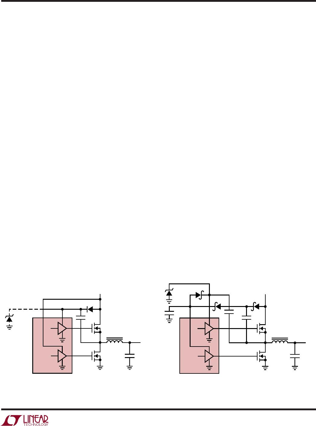
Input and Output Capacitors
A typical LTC1430 design puts significant demands on
both the input and output capacitors. Under normal steady
load operation, a buck converter like the LTC1430 draws
square waves of current from the input supply at the
switching frequency, with the peak value equal to the
output current and the minimum value near zero. Most of
this current must come from the input bypass capacitor,
since few raw supplies can provide the current slew rate to
feed such a load directly. The resulting RMS current flow
in the input capacitor will heat it up, causing premature
capacitor failure in extreme cases. Maximum RMS current
occurs with 50% PWM duty cycle, giving an RMS current
APPLICATIO S I FOR ATIO
WUU
U

LTC1430CS#TRPBF

Mfr. #:
Manufacturer:
Analog Devices / Linear Technology
Description:
Switching Voltage Regulators Hi Pwr Buck Sw Reg Cntr
Lifecycle:
New from this manufacturer.
Delivery:
DHL FedEx Ups TNT EMS
Payment:
T/T Paypal Visa MoneyGram Western Union