XR-T6166
...the analog plus company
TM
Codirectional Digital Data
Processor
Rev. 2.03
2010
EXAR Corporation, 48720 Kato Road, Fremont, CA 94538 (510) 668-7000 (510) 668-7010
1
Dec 2010
FEATURES
Low Power CMOS Technology
All Receiver and Transmitter Inputs and Outputs are
TTL Compatible
Transmitter Inhibits Bipolar Violation Insertion for
Transmission of Alarm Conditions
Alarm Output Indicates Loss of Received Bipolar
Violations
Tolerance of 125µs Variance of Data Transfer
Timing in Both Transmit and Receive Paths
Allows Operation in Plesiochronous Networks
Both Receiver and Transmitter Perform Byte
Insertion or Deletion in Response to Local Clock
Slips and Provide Outputs Indicating Slip Logic
Activity
APPLICATIONS
CCITT G.703 Compliant 64kbps Codirectional
Interface
Performs the Digital and Analog Functions for
a Complete 64kbps Data Adaption Unit (DAU) When
Used With the XR-T6164
GENERAL DESCRIPTION
The XR-T6166 is a CMOS device which contains the
digital circuitry necessary to interface both directions of a
64kbps data stream to 2.048Mbps transmit and receive
PCM time-slots. The XR-T6166 and the companion
XR-T6164 line interface chip together form a CCITT
G.703 compliant 64kbps codirectional interface.
The XR-T6166 contains separate transmit and receive
sections. The transmitter transforms 8 bit serial data from
a 2.048Mbps time-slot into an encoded 64kbps data
stream. The receiver , which performs the reverse
operation, decodes the 64kbps data, extracts a clock
signal, and then outputs the data to a 2.048Mbps
time-slot. The XR-T6166 provides features which allow
the repetitions and deletions of both received and
transmitted data as clock skews and transients occur .
These slip occurrences are indicated by byte insertion
and deletion flags. Outputs are also provided for
extracted receive clock and clock recovery circuit loss of
lock.
ORDERING INFORMATION
Part No.
Package
Operating
Temperature Range
XR-T6166CD
28 Lead 300 Mil JEDEC SOIC
0°C to +70°C
XR-T6166ID 28 Lead 300 Mil JEDEC SOIC –40°C to 85°C
XR-T6166
2
Rev. 2.03
Byte
Deletion
19
PCMIN
20
TX2MHz
10
TS1T
15
TTSEL
12
TS2T
time-slot
Mux
8 Bit Latch
8
Load
8
8 Bit Output Register
Q
Load
CLK
Byte
Insertion
11
BDT
18
BIT
13
T+R
Violation
Insertion
Coding
Logic
Octet
Counter
16
ALARMIN
Control
Circuitry
17
TX256kHz
14
T-R
CLK
CLK
D
D
Q
Q
Figure 1. XR-T6166 Transmitter Section Block Diagram
8 Bit Input Register
D
CLK
1
ALARM
Violation
Loss
Alarm
Data
Decoder
CLK
2
S+R
3
S-R
Byte Sync
Detection
CLK
5
RX2MHz
23
TS1R
4
BLS
Time
Slot
Mux
8 Bit Reg 0
D
CLK
Q
8 Bit Reg 1
D
CLK
Q
Register
Select
Logic
28
PCMOUT
26
BIR
25
BDR
Byte
Insertion
Byte
Deletion
REG 0 SEL
REG 1 SEL
time-slot
24
TS2R
27
RTSEL
6
BLANK
9
RXCK2MHz
Clock
Recovery
128kHz Recovered Clock
22
CS
7
RXCKOUT
Figure 2. XR-T6166 Receiver Section Block Diagram
time-slot
Mux
XR-T6166
3
Rev. 2.03
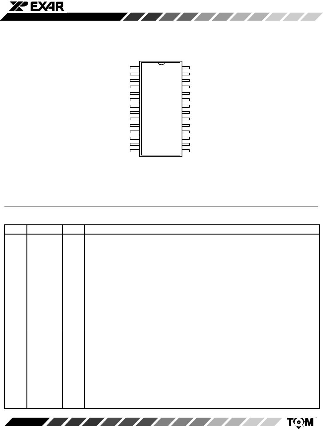
PIN CONFIGURATION
281
1514
2
3
4
5
6
7
17
16
8
9
19
18
10
11
23
22
21
20
27
26
25
24
12
13
PCMOUT
RTSEL
BIR
BDR
TS2R
TS1R
CS
V
SS
ALARM
S+R
S-R
BLS
RX2MHz
BLANK
RXCKOUT
V
DD
TX2MHz
RXCK2MHz
PCMIN
TS1T
BIT
BDT
TX256kHz
TS2T
ALARMIN
T+R
TTSEL
T-R
28 Lead SOIC (Jedec, 0.300”)
PIN DESCRIPTION
Pin # Symbol Type Description
1 ALARM O Octet Timing Alarm. When active, indicates loss of received bipolar violations that are used
for octet timing. Active high.
2 S+R I Positive AMI Data to Receiver. Positive data from the XR-T6164 receive-side. Active low.
3 S-R I Negative AMI Data to Receiver. Negative data from the XR-T6164 receive-side. Active low.
4 BLS I Byte Locking Supervision. When active, causes blanking of PCMOUT under received
alarm conditions. Active low.
5 RX2MHz I Receiver 2.048MHz Clock. Used to clock out PCM data.
6 BLANK I PCMOUT Data Blanking. When active, forces PCMOUT data to all ones (AIS). Active high.
7 RXCKOUT O 128kHz Extracted Clock. Clock recovered from received data.
8 V
DD
+5V 10% Power Source.
9 RXCK2MHz I 2.048MHz Clock. Used by receiver clock recovery circuit.
10 TS1T I Transmitter Time-slot 1 Input.
11 BDT O Transmitter Byte Deletion Flag. Active when a transmit byte is deleted. Active high.
12 TS2T I Transmitter Time-slot 2 Input.
13 T+R O Transmit Positive AMI Data Output. Data to XR-T6164 positive transmitter input. Active low.
14 T-R O Transmit Negative AMI Data Output. Data to XR-T6164 negative transmitter input. Active
low.
15 TTSEL I Transmit Time-slot Select. When high, pin 10 is selected; when low, pin 12 is selected.
16 ALARMIN I Alarm Input. When active, inhibits insertion of violations used for octet timing in transmitter
output. Active high.

XRT6166CD-F

Mfr. #:
Manufacturer:
MaxLinear
Description:
Network Controller & Processor ICs 4.5V-5.5V temp 0C to 70C
Lifecycle:
New from this manufacturer.
Delivery:
DHL FedEx Ups TNT EMS
Payment:
T/T Paypal Visa MoneyGram Western Union

Products related to this Datasheet