XR-T6166
5
Rev. 2.03
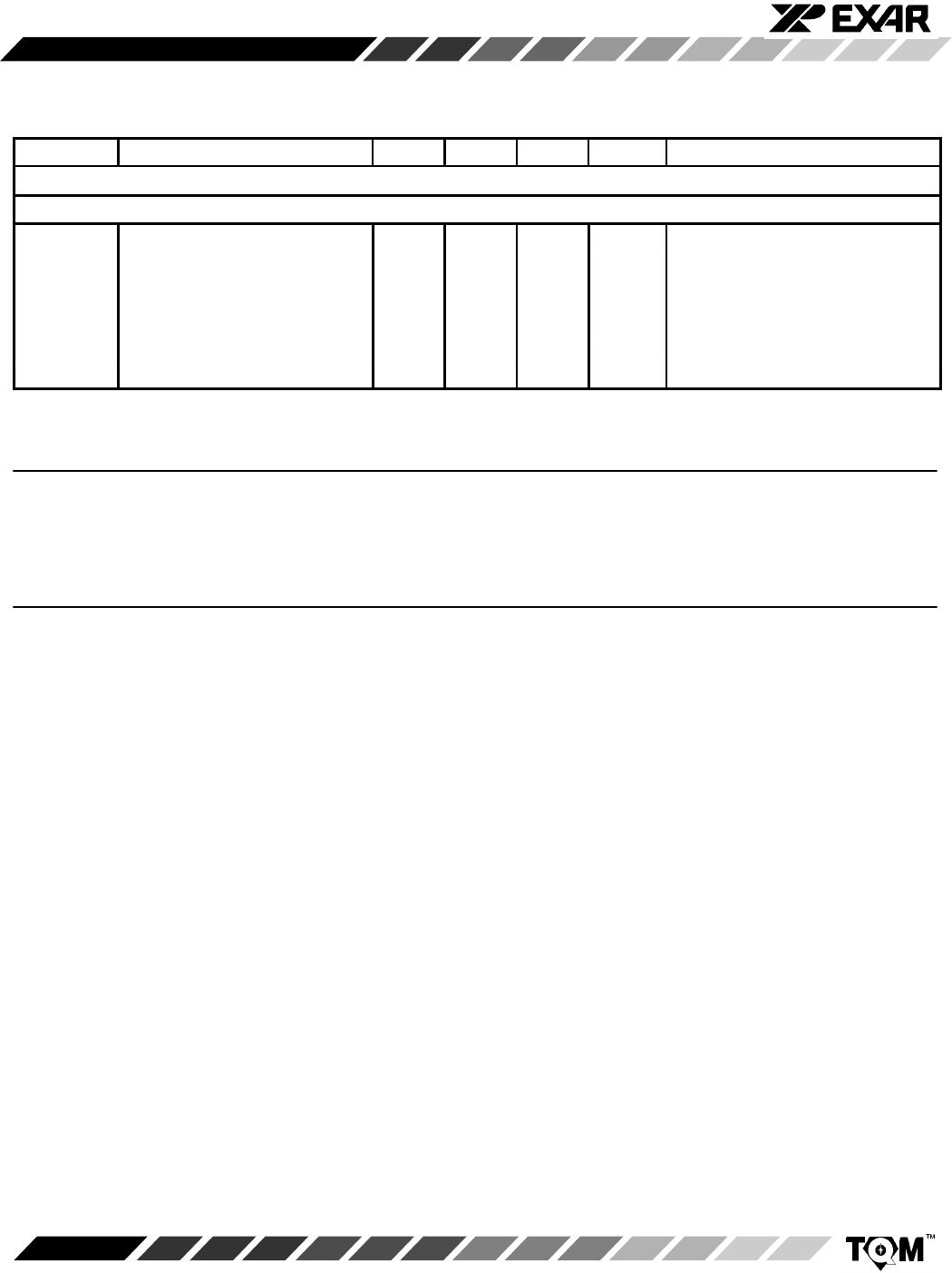
ELECTRICAL CHARACTERISTICS
Test Conditions: V
DD
= 5V 10%, T
A
= 25°C, Unless Otherwise Specified
Symbol Parameter Min. Typ. Max. Unit Conditions
DC Electrical Characteristics
V
IH
Logic 1 2.4 V
V
IL
Logic 0 0.4 V
V
DD
Supply 4.5 5.5 V
I
DD
Supply Current 500 µA Dynamic Supply Current
I
IL
Input Leakage 1 µA
V
OL
0.4 V At 1.6mA
V
OH
2.4 mA At 0.4mA
AC Electrical Characteristics
General
tr, tf Output Rise/Fall Time 20 ns All Outputs
Receiver
tRS RX2MHz Rising Edge to TS
Rising Edge Set Up Time
0 tRXL-
100
ns
Figure 3
tRH RX2MHz Rising Edge to TS
Falling Edge Hold Time
0 tRXL-
100
ns
Figure 3
tDRS TS Rising Edge to Leading Edge
of PCMOUT D0 Bit Delay
10 ns
Figure 3
tDRH TS Falling Edge to Trailing Edge
of PCMOUT D7 Bit Hold Time
0 10 ns
Figure 3
tRXD RX2MHz Rising Egde to
PCMOUT Bits D1 Through D6
Rising Edge Delay
10 ns
Figure 3
tPW PCMOUT Pulse Width 488 ns
Figure 3
tRXH RX2MHz High Time 244 ns
Figure 3
tRXL RX2MHz Low Time 244 ns
Figure 3
tRXCLK RX2MHz Period 488 ns 100ppm
Transmitter
tTS TS Rising Edge to TX2MHz Set
Up Time
20 tTXL-
100
ns
Figure 5
tTH TS Falling Edge to TX2MHz Hold
Time
0 tTXL-
100
ns
Figure 5
tDS PCMIN Edge to TX2MHz Set Up
Time
100 ns
Figure 5
tDH PCMIN Edge to TX2MHz Hold
Time
100 ns
Figure 5
tTXH TX2MHz High Time 244 ns
Figure 5
tTXL TX2MHz Low Time 244 ns
Figure 5
tTXCLK TX2MHz Period 488 ns 100ppm