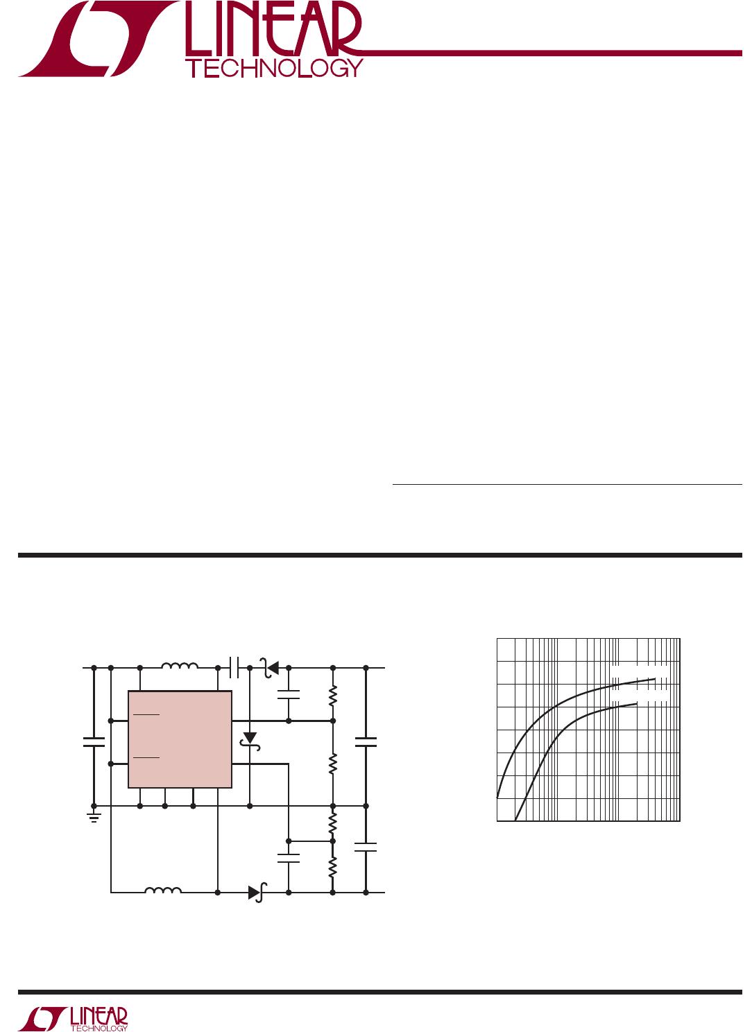
LT1945
2
1945fa
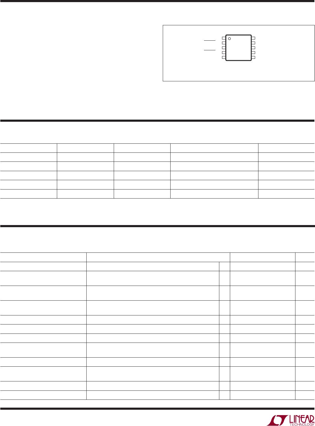
PIN CONFIGURATION ABSOLUTE MAXIMUM RATINGS
V
IN
, SHDN1, SHDN2 Voltage .....................................15V
SW1, SW2 Voltage ....................................................36V
NFB1 Voltage ............................................................–3V
FB2 Voltage ............................................................... VIN
Current into NFB1 Pin ............................................–1mA
Current into FB2 Pin ................................................1mA
Junction Temperature ........................................... 125°C
Operating Temperature Range (Note 2).... –40°C to 85°C
Storage Temperature Range ................... –65°C to 150°C
Lead Temperature (Soldering, 10 sec) .................. 300°C
(Note 1)
1
2
3
4
5
NFB1
SHDN1
GND
SHDN2
FB2
10
9
8
7
6
SW1
PGND
V
IN
PGND
SW2
TOP VIEW
MS PACKAGE
10-LEAD PLASTIC MSOP
T
JMAX
= 125°C, θ
JA
= 160°C/W
ORDER INFORMATION
LEAD FREE FINISH TAPE AND REEL PART MARKING* PACKAGE DESCRIPTION TEMPERATURE RANGE
LT1945EMS#PBF LT1945EMS#TRPBF LTTS 10-Lead Plastic MSOP –40°C to 85°C
LT1945IMS#PBF LT1945IMS#TRPBF LTTS 10-Lead Plastic MSOP –40°C to 125°C
LEAD BASED FINISH TAPE AND REEL PART MARKING* PACKAGE DESCRIPTION TEMPERATURE RANGE
LT1945EMS LT1945EMS#TR LTTS 10-Lead Plastic MSOP –40°C to 85°C
LT1945IMS LT1945IMS#TR LTTS 10-Lead Plastic MSOP –40°C to 125°C
Consult LTC Marketing for parts specifi ed with wider operating temperature ranges. *The temperature grade is identifi ed by a label on the shipping container.
For more information on lead free part marking, go to: http://www.linear.com/leadfree/
For more information on tape and reel specifi
cations, go to: http://www.linear.com/tapeandreel/
PARAMETER CONDITIONS MIN TYP MAX UNITS
Minimum Input Voltage 1.2 V
Quiescent Current, (per Converter) Not Switching
V
SHDN
= 0V
20 30
1
μA
μA
NFB1 Comparator Trip Point –40°C < T
J
< 85°C
–40°C < T
J
< 125°C
–1.205
–1.195
–1.23 –1.255
1.255
V
V
FB2 Comparator Trip Point –40°C < T
J
< 85°C
–40°C < T
J
< 125°C
1.205
1.195
1.23 1.255
1.255
V
V
FB Comparator Hysteresis 8mV
NFB1, FB2 Voltage Line Regulation 1.2V < V
IN
< 12V 0.05 0.1 %/V
NFB1 Pin Bias Current (Note 3) V
NFB1
= –1.23V
l
1.3 2 2.9 μA
FB2 Pin Bias Current (Note 4) –40°C < T
J
< 85°C
–40°C < T
J
< 125°C
30 80
300
nA
nA
Switch Off Time, Switcher 1 (Note 5) 400 ns
Switch Off Time, Switcher 2 (Note 5) V
FB2
> 1V
V
FB2
< 0.6V
400
1.5
ns
μs
Switch V
CESAT
I
SW
= 300mA 250 350 mV
Switch Current Limit
250 350 400 mA
ELECTRICAL CHARACTERISTICS
The l denotes the specifi cations which apply over the full operating
temperature range, otherwise specifi cations are at T
A
= 25°C. V
IN
= 1.2V, V
SHDN
= 1.2V unless otherwise noted.