LT1945
7
1945fa
Information furnished by Linear Technology Corporation is believed to be accurate and reliable.
However, no responsibility is assumed for its use. Linear Technology Corporation makes no representa-
tion that the interconnection of its circuits as described herein will not infringe on existing patent rights.
APPLICATIONS INFORMATION
of related parts.
Table 2. Recommended Capacitors
CAPACITOR TYPE VENDOR
Ceramic Taiyo Yuden
(408) 573-4150
www.t-yuden.com
Ceramic AVX
(803) 448-9411
www.avxcorp.com
Ceramic Murata
(714) 852-2001
www.murata.com
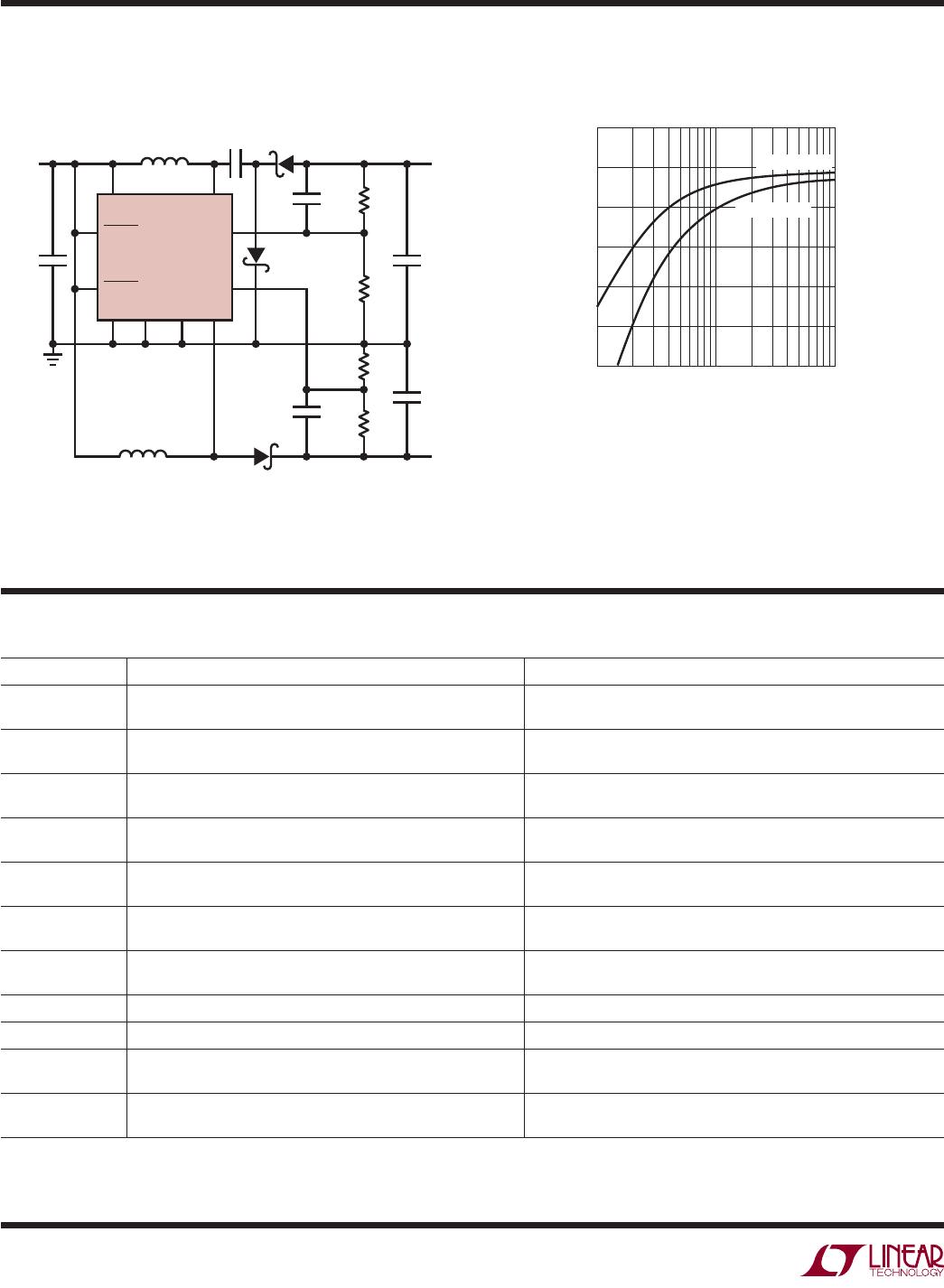
Setting the Output Voltages
Set the output voltage for Switcher 1 (negative output
voltage ) by choosing the appropriate values for feedback
resistors R1 and R2.
R
VV
V
R
OUT
1
123
123
2
210
6
=
+
()
−
–.
.
•
Set the output voltage for Switcher 2 (positive output
voltage) by choosing the appropriate values for feedback
resistors R1B and R2B (see Figure 1).
RR
V
OUT
12
123
1=−
⎛
⎝
⎜
⎞
⎠
⎟
.
Diode Selection
For most LT1945 applications, the Zetex ZHCS400 sur-
face mount Schottky diode (0.4A, 40V) is an ideal choice.
Schottky diodes, with their low forward voltage drop and
fast switching speed, are the best match for the LT1945.
The Motorola MBR0520, MBR0530, or MBR0540 can also
be used. Many different manufacturers make equivalent
parts, but make sure that the component is rated to handle
at least 0.35A.
Lowering Output Voltage Ripple
Using low ESR capacitors will help minimize the output
ripple voltage, but proper selection of the inductor and the
output capacitor also plays a big role. The LT1945 provides
energy to the load in bursts by ramping up the inductor
current, then delivering that current to the load. If too large
of an inductor value or too small of a capacitor value is
used, the output ripple voltage will increase because the
capacitor will be slightly overcharged each burst cycle.
To reduce the output ripple, increase the output capacitor
value or add a 4.7pF feed-forward capacitor in the feedback
network of the LT1945 (see the circuits in the Typical Ap-
plications section). Adding this small, inexpensive 4.7pF
capacitor will greatly reduce the output voltage ripple.
PACKAGE DESCRIPTION
MS Package
10-Lead Plastic MSOP
(Reference LTC DWG # 05-08-1661)
MSOP (MS) 0402
0.53 p 0.01
(.021 p .006)
SEATING
PLANE
0.18
(.007)
1.10
(.043)
MAX
0.17 –0.27
(.007 – .011)
0.13 p 0.05
(.005 p .002)
0.86
(.034)
REF
0.50
(.0197)
TYP
12
3
45
4.88 p 0.10
(.192 p .004)
0.497 p 0.076
(.0196 p .003)
REF
8910
7
6
3.00 p 0.102
(.118 p .004)
(NOTE 3)
3.00 p 0.102
(.118 p .004)
NOTE 4
NOTE:
1. DIMENSIONS IN MILLIMETER/(INCH)
2. DRAWING NOT TO SCALE
3. DIMENSION DOES NOT INCLUDE MOLD FLASH, PROTRUSIONS OR GATE BURRS.
MOLD FLASH, PROTRUSIONS OR GATE BURRS SHALL NOT EXCEED 0.152mm (.006") PER SIDE
4. DIMENSION DOES NOT INCLUDE INTERLEAD FLASH OR PROTRUSIONS.
INTERLEAD FLASH OR PROTRUSIONS SHALL NOT EXCEED 0.152mm (.006") PER SIDE
5. LEAD COPLANARITY (BOTTOM OF LEADS AFTER FORMING) SHALL BE 0.102mm (.004") MAX
0.254
(.010)
0
o – 6o TYP
DETAIL “A”
DETAIL “A”
GAUGE PLANE
5.23
(.206)
MIN
3.2 – 3.45
(.126 – .136)
0.889 p 0.127
(.035 p .005)
RECOMMENDED SOLDER PAD LAYOUT
0.305 p 0.038
(.0120 p .0015)
TYP
0.50
(.0197)
BSC