IRS2982SPBF
16 2017-02-07
t
twd
V(t)
VOUT(t)
VZX(t)
VCOMP(t)
Figure 6: Overvoltage protection
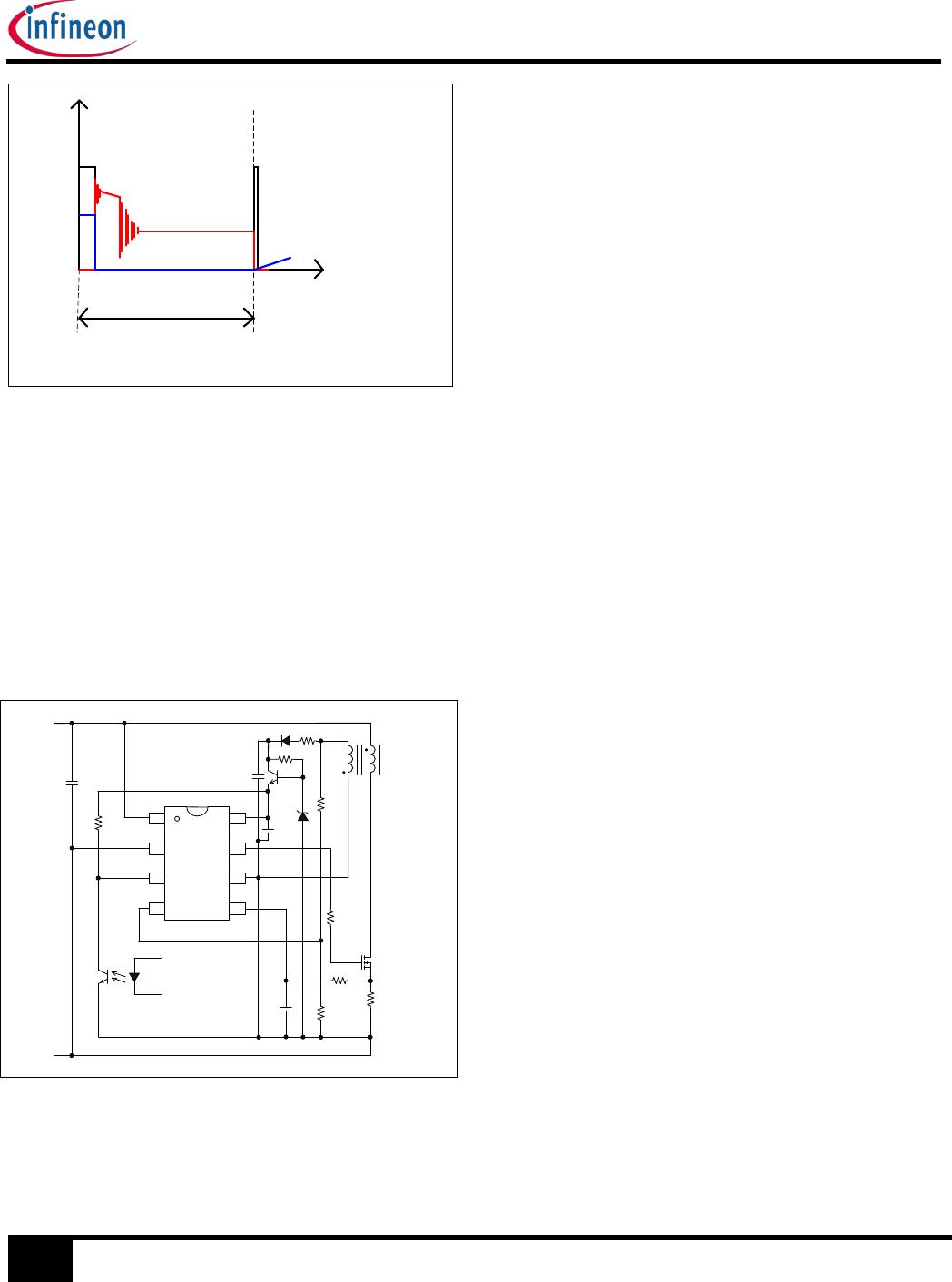
Operating with a secondary feedback circuit
In applications where galvanic isolation and
accurate voltage and/or current regulation are
required, the IRS2982 should be used in
conjunction with a secondary sensing and
feedback circuit. The feedback circuit is fed
through an opto-isolator connected to the IRS2982
as follows:
A simple feedback scheme is shown in figure 7 to
illustrate how an opto-isolator may be connected
to the IRS2982 to create a feedback circuit. The
FB input is tied to COM leaving the error amplifier
inverting input at zero volts so that the COMP
output provides pull up. The opto-isolator feedback
pulls down on the COMP voltage to reduce the on
time as the opto-diode current is increased driven
by a secondary error amplifier circuit typically
based around the TL431 IC. A pull-up resistor
from COMP to VCC and a capacitor from COMP
to 0V are recommended for optimum stability.
The IRS2982 remains in start mode since the FB
input is connected to 0V and can therefore never
rise above the V
REG
threshold to enter regulation
mode. Operation in start mode is possible,
however VCC should be set to 17V or higher to
ensure that only micro current is drawn from the
high voltage regulator during steady state
operation. This is easily done by using a series
pass transistor (QVCC) with the base biased with
an 18V zener diode (DZX) to supply VCC. Care
should be taken to avoid auxiliary winding voltages
above 25V to prevent overheating of QVCC.
T1
CIN
MPFC
RPFC
RCS
CF2
RF
DVCC
IC1
RZX1
RZX2
CVCC2
Secondary error
feedback
DZX
QVCC
RVCC2
RVCC1
CVCC1
RPU
CS
COM
OUT
VCC
COMP
FB
HV
ZX
IRS2982
7
6
5
1
2
3
4
8
Figure 7: Secondary feedback circuit opto-isolator
connection
Performance Graphs