MAX9725
1V, Low-Power, DirectDrive, Stereo Headphone
Amplifier with Shutdown
_______________________________________________________________________________________ 7
PIN BUMP
THIN
QFN
UCSP
NAME FUNCTION
1 A1 C1N Flying Capacitor Negative Terminal. Connect a 1µF capacitor from C1P to C1N.
2A2PV
SS
Inverting Charge-Pump Output. Bypass with 1µF from PV
SS
to PGND. PV
SS
must be connected to
V
SS
.
3 A3 INL
Left-Amplifier Inverting Input. Connect input resistor R
IN
from input capacitor C1N to INL (MAX9725E
only).
4 A4 INR
Right-Amplifier Inverting Input. Connect input resistor R
IN
from input capacitor C1N to INR
(MAX9725E only).
5B4V
SS
Amplifier Negative Power Supply. Must be connected to PV
SS
.
6 B3 SGND
Signal Ground. SGND must be connected to PGND. SGND is the ground reference for the input and
output signal.
7 C4 OUTR Right-Channel Output. Connect feedback resistor R
FB
between OUTR and INR (MAX9725E only).
8 C3 OUTL Left-Channel Output. Connect feedback resistor R
FB
between OUTL and INL (MAX9725E only).
9C2V
DD
Positive Power-Supply Input. Bypass with a 1µF capacitor to PGND.
10 C1 C1P Flying Capacitor Positive Terminal. Connect a 1µF capacitor from C1P to C1N.
11 B1 PGND Power Ground. Ground reference for the internal charge pump. PGND must be connected to SGND.
12 B2 SHDN
Active-Low Shutdown. Connect to V
DD
for normal operation. Pull low to disable the amplifier and
charge pump.
EP EP Exposed Paddle. Internally connected to V
SS
. Leave paddle unconnected or solder to V
SS
.
Pin Description
SHUTDOWN CURRENT
vs. SUPPLY VOLTAGE
MAX9725 toc22
SUPPLY VOLTAGE (V)
SHUTDOWN CURRENT (μA)
1.31.1
0.1
0.2
0.3
0.4
0.5
0.6
0.7
0
0.9 1.5
EXITING SHUTDOWN
MAX9725 toc23
200μs/div
OUT_
1V/div
SHDN
500mV/div
POWER-UP/-DOWN WAVEFORM
MAX9725toc24
200ms/div
OUT_
10mV/div
V
DD
1V/div
Typical Operating Characteristics (continued)
(V
DD
= 1.5V, V
PGND
= V
SGND
= 0V, V
SHDN
= 1.5V, V
SS
= V
PVSS,
C1 = C2 = 1µF, C
IN
= 1µF, THD+N measurement bandwidth = 22Hz
to 22kHz, T
A
= +25°C, unless otherwise noted.) (See the
Functional Diagrams.
)
MAX9725
1V, Low-Power, DirectDrive, Stereo Headphone
Amplifier with Shutdown
8 _______________________________________________________________________________________
Detailed Description
The MAX9725 stereo headphone driver features Maxim’s
DirectDrive architecture, eliminating the large output-cou-
pling capacitors required by conventional single-supply
headphone drivers. The MAX9725 consists of two 20mW
class AB headphone drivers, shutdown control, inverting
charge pump, internal gain-setting resistors, and compre-
hensive click-and-pop suppression circuitry (see the
Functional Diagrams
). A negative power supply (PV
SS
) is
created by inverting the positive supply (V
DD
). Powering
the drivers from V
DD
and PV
SS
increases the dynamic
range of the drivers to almost twice that of other 1V sin-
gle-supply drivers. This increase in dynamic range allows
for higher output power.
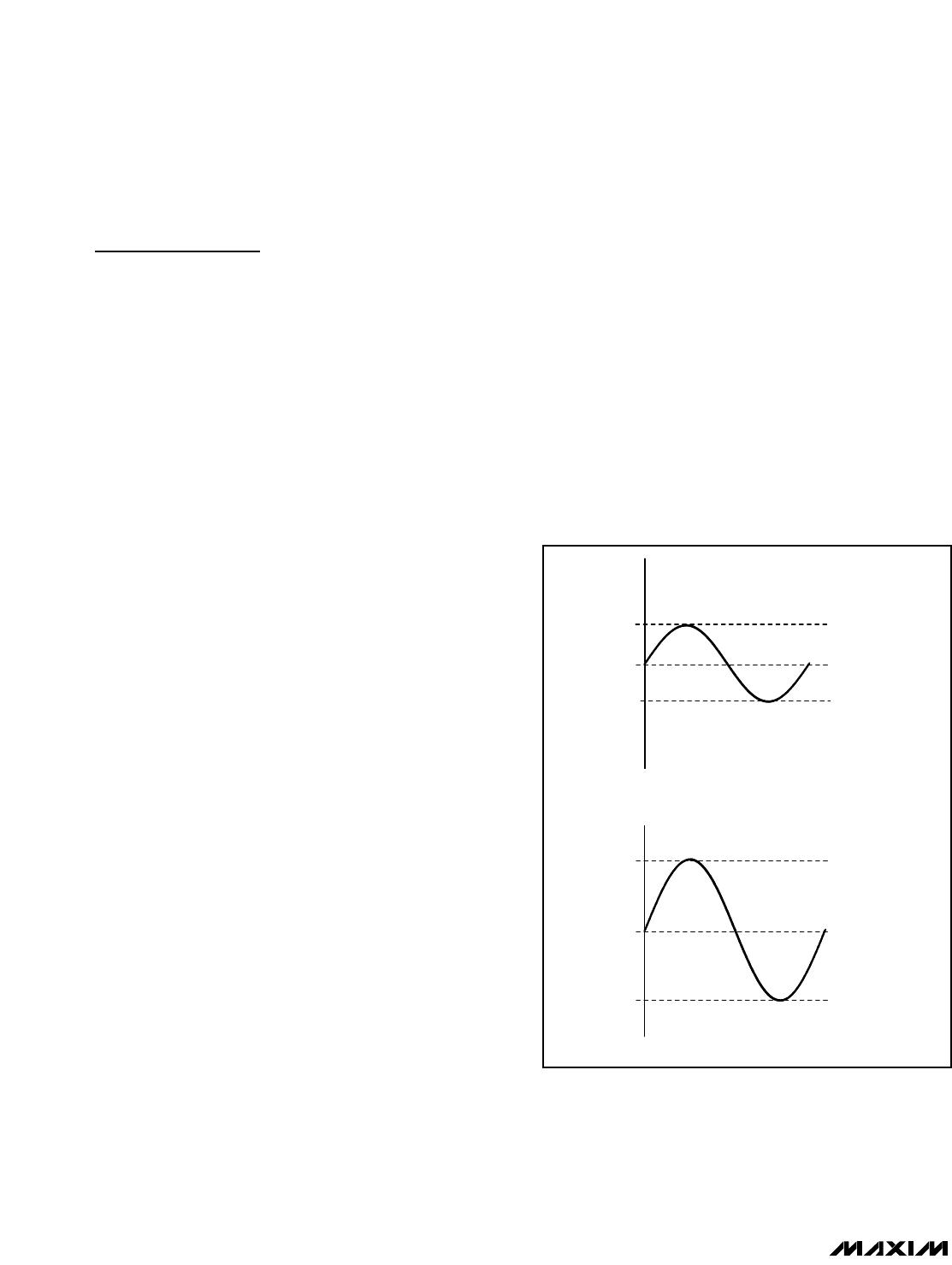
The outputs of the MAX9725 are biased about GND
(Figure 1). The benefit of this GND bias is that the driver
outputs do not have a DC component, thus large DC-
blocking capacitors are unnecessary. Eliminating the
DC-blocking capacitors on the output saves board
space, system cost, and improves frequency response.
DirectDrive
Conventional single-supply headphone drivers have their
outputs biased about a nominal DC voltage (typically half
the supply) for maximum dynamic range. Large coupling
capacitors are needed to block the DC bias from the
headphones. Without these capacitors, a significant
amount of DC current flows to the headphone, resulting
in unnecessary power dissipation and possible damage
to both headphone and headphone driver.
Maxim’s DirectDrive architecture uses a charge pump
to create an internal negative supply voltage. This
allows the MAX9725 outputs to be biased about GND,
increasing the dynamic range while operating from a
single supply. A conventional amplifier powered from
1.5V ideally provides 18mW to a 16Ω load. The
MAX9725 provides 25mW to a 16Ω load. The
DirectDrive architecture eliminates the need for two
large (220µF, typ) DC-blocking capacitors on the out-
put. The MAX9725 charge pump requires two small
ceramic capacitors, conserving board space, reducing
cost, and improving the frequency response of the
headphone driver. See the Output Power vs. Charge-
Pump Capacitance and Load Resistance graph in the
Typical Operating Characteristics
for details of the possi-
ble capacitor sizes.
Previous attempts to eliminate the output-coupling
capacitors involved biasing the headphone return
(sleeve) to the DC-bias voltage of the headphone
amplifiers. This method raises some issues:
The sleeve is typically grounded to the chassis.
Using this biasing approach, the sleeve must be
isolated from system ground, complicating product
design.
During an ESD strike, the driver’s ESD structures
are the only path to system ground. The driver must
be able to withstand the full ESD strike.
When using the headphone jack as a line out to
other equipment, the bias voltage on the sleeve may
conflict with the ground potential from other equip-
ment, resulting in possible damage to the drivers.
Figure 1. Traditional Driver Output Waveform vs. MAX9725
Output Waveform (Ideal Case)
V
DD
-V
DD
GND
V
OUT
CONVENTIONAL DRIVER-BIASING SCHEME
DirectDrive BIASING SCHEME
V
DD
/ 2
V
DD
GND
V
OUT
MAX9725
Low-Frequency Response
Large DC-blocking capacitors limit the amplifier’s low-
frequency response and can distort the audio signal:
1) The impedance of the headphone load and the DC-
blocking capacitor forms a highpass filter with the
-3dB point set by:
where R
L
is the impedance of the headphone and
C
OUT
is the value of the DC-blocking capacitor. The
highpass filter is required by conventional single-
ended, single power-supply headphone drivers to
block the midrail DC-bias component of the audio
signal from the headphones. The drawback to the
filter is that it can attenuate low-frequency signals.
Larger values of C
OUT
reduce this effect but result
in physically larger, more expensive capacitors.
Figure 2 shows the relationship between the size of
C
OUT
and the resulting low-frequency attenuation.
Note that the -3dB point for a 16Ω headphone with
a 100µF blocking capacitor is 100Hz, well within the
normal audio band, resulting in low-frequency
attenuation of the reproduced signal.
2) The voltage coefficient of the DC-blocking capacitor
contributes distortion to the reproduced audio signal
as the capacitance value varies when the function of
the voltage across the capacitor changes. At low
frequencies, the reactance of the capacitor domi-
nates at frequencies below the -3dB point and the
voltage coefficient appears as frequency-dependent
distortion. Figure 3 shows the THD+N introduced by
two different capacitor dielectric types. Note that
below 100Hz, THD+N increases rapidly.
The combination of low-frequency attenuation and fre-
quency-dependent distortion compromises audio
reproduction in portable audio equipment that empha-
sizes low-frequency effects such as multimedia lap-
tops, as well as MP3, CD, and DVD players. These
low-frequency, capacitor-related deficiencies are elimi-
nated by using DirectDrive technology.
Charge Pump
The MAX9725 features a low-noise charge pump. The
580kHz switching frequency is well beyond the audio
range, and does not interfere with the audio signals.
The switch drivers feature a controlled switching speed
that minimizes noise generated by turn-on and turn-off
transients. The di/dt noise caused by the parasitic bond
wire and trace inductance is minimized by limiting the
turn-on/off speed of the charge pump. Additional high-
frequency noise attenuation can be achieved by
increasing the size of C2 (see the
Functional Diagrams
).
Extra noise attenuation is not typically required.
Shutdown
The MAX9725’s low-power shutdown mode reduces
supply current to 0.6µA. Driving SHDN low disables the
amplifiers and charge pump. The driver’s output imped-
ance is typically 50kΩ (MAX9725A), 37.5kΩ
(MAX9725B), 25kΩ (MAX9725C), 100kΩ (MAX9725D),
or R
F
(MAX9725E) when in shutdown mode.
f
2RC
-3dB
L OUT
=
1
π
Figure 2. Low-Frequency Attenuation for Common DC-Blocking
Capacitor Values
LF ROLLOFF (16Ω LOAD)
FREQUENCY (Hz)
ATTENUATION (dB)
100
-30
-25
-20
-10
-3dB CORNER FOR
100
μ
F IS 100Hz
-15
-5
-3
0
-35
10 1k
33
μ
F
330
μ
F
220
μ
F
100
μ
F
Figure 3. Distortion Contributed By DC-Blocking Capacitors
ADDITIONAL THD+N DUE
TO DC-BLOCKING CAPACITORS
FREQUENCY (Hz)
THD+N (%)
10k1k100
0.001
0.01
0.1
1
10
0.0001
10 100k
TANTALUM
ALUM/ELEC
1V, Low-Power, DirectDrive, Stereo Headphone
Amplifier with Shutdown
_______________________________________________________________________________________ 9

MAX9725DETC+

Mfr. #:
Manufacturer:
Maxim Integrated
Description:
Audio Amplifiers 1V DirectDrive Headphone Amplifier
Lifecycle:
New from this manufacturer.
Delivery:
DHL FedEx Ups TNT EMS
Payment:
T/T Paypal Visa MoneyGram Western Union