HMC8325 Data Sheet
Rev. 0 | Page 4 of 16
ABSOLUTE MAXIMUM RATINGS
Table 2.
Parameter Rating
Drain Bias Voltage (V
D1
to V
D4
) 4.5 V
Gate Bias Voltage (V
G1
to V
G4
) −3 V to 0 V
Maximum Junction Temperature (to
Maintain 1 Million Hours Mean Time to
Failure (MTTF))
175°C
Storage Temperature Range −65°C to +150°C
Operating Temperature Range −55°C to +85°C
ESD Sensitivity, Human Body Model (HBM) Class 0 (150 V)
Stresses at or above those listed under Absolute Maximum
Ratings may cause permanent damage to the product. This is a
stress rating only; functional operation of the product at these
or any other conditions above those indicated in the operational
section of this specification is not implied. Operation beyond
the maximum operating conditions for extended periods may
affect product reliability.
THERMAL RESISTANCE
Thermal performance is directly linked to printed circuit board
(PCB) design and operating environment. Careful attention to
PCB thermal design is required.
Table 3. Thermal Resistance
Package Type
θ
JC
1
Unit
C-22-1
2
225 °C/W
1
Based on ABLEBOND® 84-1LMIT as die attach epoxy.
2
Test Condition: Thermal impedance simulated values are based on
JEDEC 2S2P thermal test board with four thermal vias. See JEDEC JESD51.
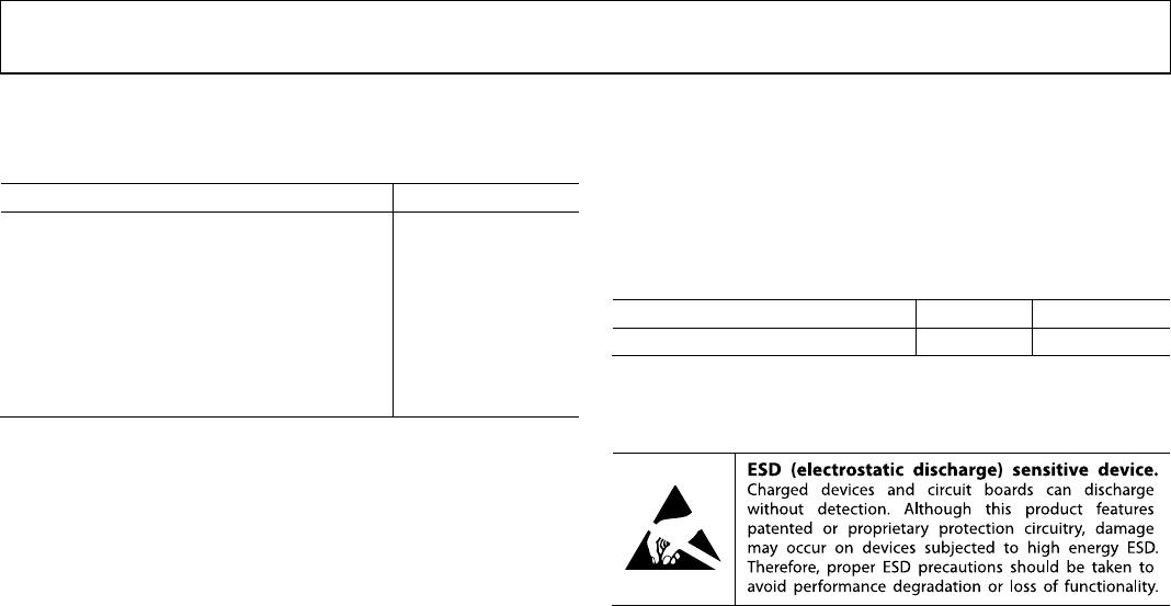
ESD CAUTION
Data Sheet HMC8325
Rev. 0 | Page 5 of 16
PIN CONFIGURATION AND FUNCTION DESCRIPTIONS
RF
OUT
RF
IN
V
G1
V
D1
V
D2
V
G2
V
D3
V
G3
V
D4
V
G4
1
2
3
4 5 6 7 8 9 10 11 12 13 14 15 16 17 18 19
20
21
22
GND
GND GND GND GND GND GND GND GND
GND
GND
GND
14692-002
HMC8325
Figure 2. Pin Configuration
Table 4. Pin Function Descriptions
Pad No. Mnemonic Description
1, 3, 4, 6, 8, 10, 12, 14, 16, 18, 20, 22 GND Ground Connection.
2 RF
IN
RF Input. AC couple RF
IN
and match it to 50 Ω.
5, 9, 13, 17 V
G1
to V
G4
Gate Bias Voltage for the Low Noise Amplifier.
7, 11, 15, 19 V
D1
to V
D4
Drain Bias Voltage for the Low Noise Amplifier.
21 RF
OUT
RF Output. AC couple RF
OUT
and match it to 50 Ω.
Die Bottom GND Ground. Die bottom must be connected to the RF/dc ground.
INTERFACE SCHEMATICS
GND
14692-003
Figure 3. GND Interface Schematic
RF
IN
14692-004
Figure 4. RF
IN
Interface Schematic
V
G1
, V
G2
, V
G3
, V
G4
14692-005
Figure 5. V
G1
to V
G4
Interface Schematic
V
D1
, V
D2
, V
D3
, V
D4
14692-006
Figure 6. V
D1
to V
D4
Interface Schematic
RF
OUT
14692-007
Figure 7. RF
OUT
Interface Schematic
HMC8325 Data Sheet
Rev. 0 | Page 6 of 16
TYPICAL PERFORMANCE CHARACTERISTICS
30
–30
65
90
89
88
87
86
85
84
83
82
81
80
79
78
77
76
75
74
73
72
71
70
69
68
67
66
GAIN AND RETURN LOSS (dB)
FREQUENCY (GHz)
–25
–20
–15
–10
–5
0
5
10
15
20
25
GAIN
INPUT RETURN LOSS
OUTPUT RETURN LOSS
14692-008
Figure 8. Gain and Return Loss vs. Frequency, V
Dx
= 3 V, I
Dx
= 57 mA
20
0
71 86
OUTPUT P1dB (dBm)
FREQUENCY (GHz)
T
A
= +85°C
T
A
= +25°C
T
A
= –55°C
2
4
6
8
10
12
14
16
18
72 73
74 75
76
77 78 79 80 81 82 83 84 85
14692-009
Figure 9. Output P1dB vs. Frequency over Temperature,
V
Dx
= 3 V, I
Dx
= 50 mA
10
–10
71 86
INPUT IP3 (dBm)
FREQUENCY (GHz)
T
A
= +85°C
T
A
= +25°C
T
A
= –55°C
72 73 74
75 76 77 78 79 80 81 82 83 84
85
–8
–6
–4
–2
0
2
4
6
8
14692-010
Figure 10. Input Third-Order Intercept (IP3) vs. Frequency over Temperatures,
P
OUT
= 5 dBm/Tone, V
Dx
= 3 V, I
Dx
= 50 mA
10
0
71 86
NOISE FIGURE (dB)
FREQUENCY (GHz)
T
A
= +85°C
T
A
= +25°C
T
A
= –55°C
72 73 74 75 76 77 78 79 80 81 82 83 84 85
1
2
3
4
5
6
7
8
9
14692-011
Figure 11. Noise Figure vs. Frequency over Temperature,
V
Dx
= 3 V, I
Dx
= 50 mA
20
10
71 86
P
SAT
(dBm)
FREQUENCY (GHz)
T
A
= +85°C
T
A
= +25°C
T
A
= –55°C
72 73 74 75 76 77 78 79 80 81 82 83 84 85
11
12
13
14
15
16
17
18
19
14692-012
Figure 12. Saturated Output Power (P
SAT
) vs. Frequency over Temperature,
V
Dx
= 3 V, I
Dx
= 50 mA
–40
–66
REVERSE ISOLATION (dB)
–64
–62
–60
–58
–56
–54
–52
–50
–48
–46
–44
–42
71 86
FREQUENCY (GHz)
T
A
= +85°C
T
A
= +25°C
T
A
= –55°C
72 73 74 75 76 77 78 79 80 81 82 83 84 85
14692-013
Figure 13. Reverse Isolation vs. Frequency over Temperature,
V
Dx
= 3 V, I
Dx
= 57 mA

HMC8325-SX

Mfr. #:
Manufacturer:
Analog Devices Inc.
Description:
RF Amplifier E-Band Low Noise Amplifier 71 to 86 GHz
Lifecycle:
New from this manufacturer.
Delivery:
DHL FedEx Ups TNT EMS
Payment:
T/T Paypal Visa MoneyGram Western Union

Products related to this Datasheet