ICS9DB803D
EIGHT OUTPUT DIFFERENTIAL BUFFER FOR PCIE GEN1 AND GEN2
IDT®
EIGHT OUTPUT DIFFERENTIAL BUFFER FOR PCIE GEN1 AND GEN2 10
ICS9DB803D REV N 071013
Clock Periods–Differential Outputs with Spread Spectrum Enabled
Clock Periods–Differential Outputs with Spread Spectrum Disabled
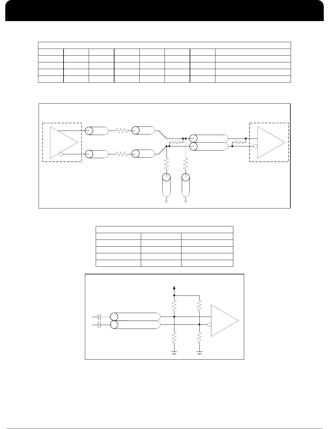
1 Clock 1us 0.1s 0.1s 0.1s 1us 1 Clock
Lg- -SSC -ppm error 0ppm + ppm error +SSC Lg+
Absolute
Period
Avera
e
Avera
e
Avera
e
Avera
e
Period
Minimum
Absolute
Period
Minimum
Absolute
Period
Minimum
Absolute
Period
Nominal Maximum Maximum Maximum
DIF 100
9.87400 9.99900 9.99900 10.00000 10.00100 10.05130 10.17630 ns 1,2,3
DIF 133
7.41425 7.49925 7.49925 7.50000 7.50075 7.53845 7.62345 ns 1,2,4
DIF 166
5.91440 5.99940 5.99940 6.00000 6.00060 6.03076 6.11576 ns 1,2,4
DIF 200
4.91450 4.99950 4.99950 5.00000 5.00050 5.02563 5.11063 ns 1,2,4
DIF 266
3.66463 3.74963 3.74963 3.75000 3.75038 3.76922 3.85422 ns 1,2,4
DIF 333
2.91470 2.99970 2.99970 3.00000 3.00030 3.01538 3.10038 ns 1,2,4
DIF 400
2.41475 2.49975 2.49975 2.50000 2.50025 2.51282 2.59782 ns 1,2,4
Notes
Units
Signal Name
Measurement
Window
Symbol
1 Clock 1us 0.1s 0.1s 0.1s 1us 1 Clock
Lg- -SSC -ppm error 0ppm + ppm error +SSC Lg+
Absolute
Period
Avera
e
Avera
e
Avera
e
Avera
e
Period
Minimum
Absolute
Period
Minimum
Absolute
Period
Minimum
Absolute
Period
Nominal Maximum Maximum Maximum
DIF 100
9.87400 9.99900 10.00000 10.00100 10.17630 ns 1,2,3
DIF 133
7.41425 7.49925 7.50000 7.50075 7.62345 ns 1,2,4
DIF 166
5.91440 5.99940 6.00000 6.00060 6.11576 ns 1,2,4
DIF 200
4.91450 4.99950 5.00000 5.00050 5.11063 ns 1,2,4
DIF 266
3.66463 3.74963 3.75000 3.75038 3.85422 ns 1,2,4
DIF 333
2.91470 2.99970 3.00000 3.00030 3.10038 ns 1,2,4
DIF 400
2.41475 2.49975 2.50000 2.50025 2.59782 ns 1,2,4
1
Guaranteed by design and characterization, not 100% tested in production.
Driven by SRC output of main clock, PLL or Bypass mode
4
Driven by CPU output of CK410/CK505 main clock,
B
ass mode onl
2
All Long Term Accuracy specifications are guaranteed with the assumption that the input clock complies with
CK409/CK410/CK505 accuracy requirements. The 9DB403/803 itself does not contribute to ppm error.
Notes
Units
Symbol
Definition
Signal Name