Features
• Programmable 16,777,216 x 1-bit Serial Memories Designed to Store Configuration
Programs for Field Programmable Gate Arrays (FPGAs)
• 3.3V Output Capability
• 5V Tolerant I/O Pins
• Program Support using the Atmel ATDH2200E System or Industry Third-party
Programmers
• In-System Programmable (ISP) via 2-wire Bus
• Simple Interface to SRAM FPGAs
• Compatible with Atmel AT40K and AT94K Devices, Altera
®
FLEX
®
, APEX
™
Devices,
Lucent
®
ORCA
®
FPGAs, Xilinx
®
XC3000, XC4000, XC5200, Spartan
®
, Virtex
®
FPGAs,
Motorola
®
MPA1000 FPGAs
• Cascadable Read-back to Support Additional Configurations or Higher-density Arrays
• Low-power CMOS FLASH Process
• Available in 6 mm x 6 mm x 1 mm 8-lead LAP (Pin-compatible with 8-lead SOIC/VOIC
Footprint Packages), 20-lead PLCC and 44-lead TQFP Packages
• Emulation of Atmel’s AT24CXXX Serial EEPROMs
• Low-power Standby Mode
• Single Device Capable of Holding 4-bit Stream Files Allowing Simple System
Reconfiguration
• Fast Serial Download Speeds up to 33 MHz
• Endurance: 10,000 Write Cycles Typical
• Green (Pb/Halide-free/RoHS Compliant) Package Options Available
1. Description
The AT17F Series of In-System Programmable Configuration PROMs (Configurators)
provide an easy-to-use, cost-effective configuration memory for Field Programmable
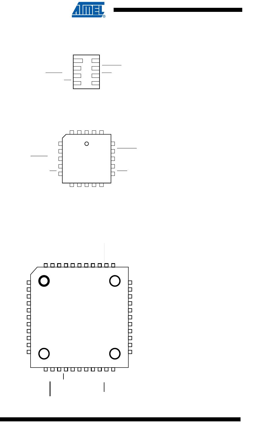
Gate Arrays. The AT17F Series device is packaged in the 8-lead LAP, 20-lead PLCC
and 44-lead TQFP, see Table 1-1. The AT17F Series Configurator uses a simple
serial-access procedure to configure one or more FPGA devices.
The AT17F Series Configurators can be programmed with industry-standard program-
mers, Atmel’s ATDH2200E Programming Kit or Atmel’s ATDH2225 ISP Cable.
Table 1-1. AT17F Series Packages
Package AT17F16
8-lead LAP Yes
20-lead PLCC Yes
44-lead TQFP Yes
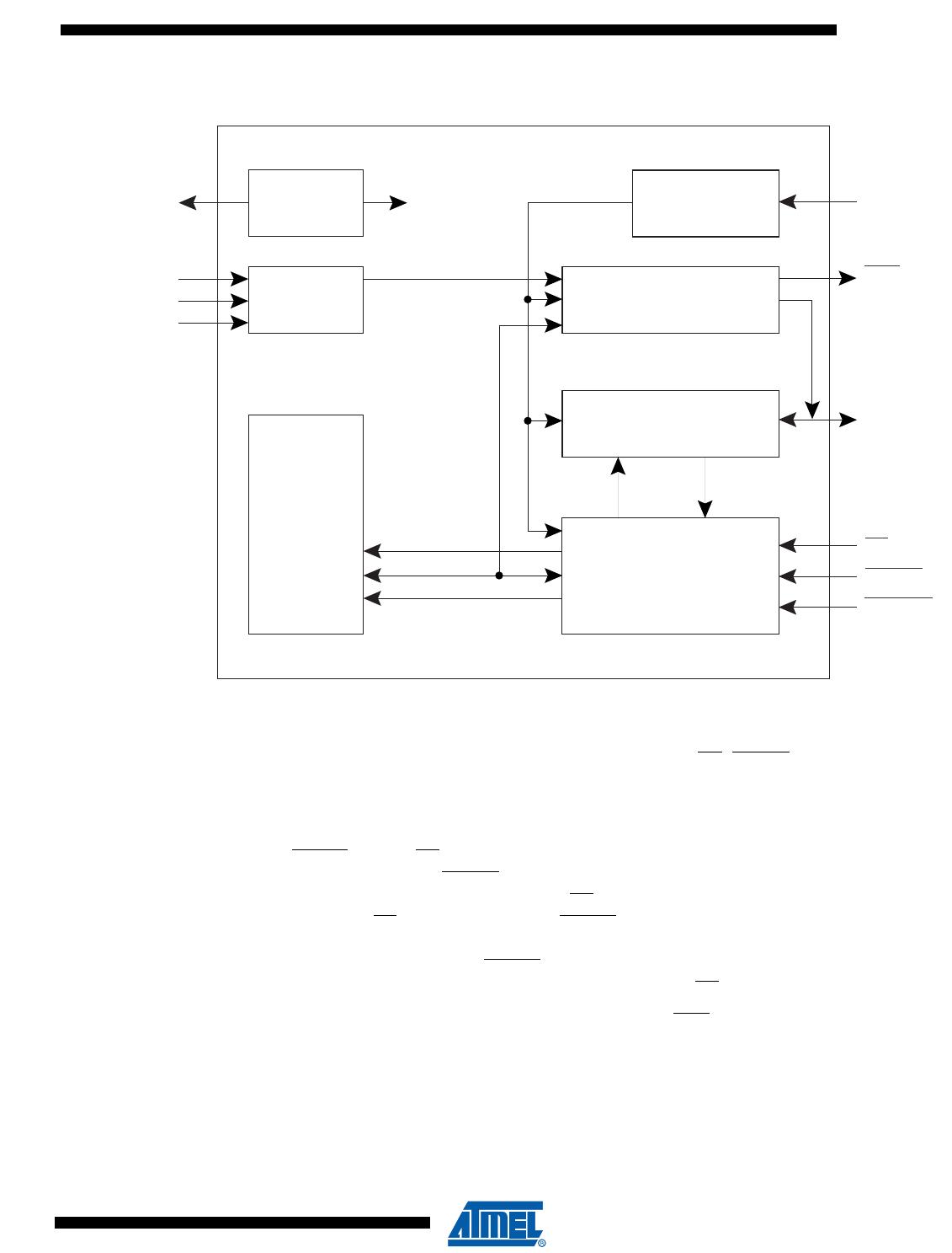
FPGA
Configuration
Flash Memory
AT17F16
3392F–CNFG–2/08