5
3392F–CNFG–2/08
AT17F16
5.4 PAGESEL[1:0]
(2)
Page select inputs. Used to determine which of the 4 memory pages are targeted during a serial
configuration download. The address space for each of the pages is shown in Table 5-2. When
SER_EN
is Low (ISP mode) these pins have no effect.
5.5 RESET/OE
(1)
Output Enable (active High) and RESET (active Low) when SER_EN is High. A Low level on
RESET/OE resets both the address and bit counters. A High level (with CE Low) enables the
data output driver.
5.6 CE
(1)
Chip Enable input (active Low). A Low level (with OE High) allows CLK to increment the address
counter and enables the data output driver. A High level on CE
disables both the address and bit
counters and forces the device into a low-power standby mode. Note that this pin will not
enable/disable the device in the 2-wire Serial Programming mode (SER_EN Low).
5.7 GND
Ground pin. A 0.2 µF decoupling capacitor between V
CC
and GND is recommended.
5.8 CEO
Chip Enable Output (when SER_EN is High). This output goes Low when the internal address
counter has reached its maximum value. If the PAGE_EN input is set High, the maximum value
is the highest address in the selected partition. The PAGESEL[1:0] inputs are used to make the
4 partition selections. If the PAGE_EN input is set Low, the device is not partitioned and the
address maximum value is the highest address in the device, see Table 5-2 on page 5. In a
daisy chain of AT17F Series devices, the CEO
pin of one device must be connected to the CE
input of the next device in the chain. It will stay Low as long as CE is Low and OE is High. It will
then follow CE until OE goes Low; thereafter, CEO will stay High until the entire EEPROM is
read again.
5.9 A2
(1)
Device selection input, (when SER_EN Low). The input is used to enable (or chip select) the
device during programming (i.e., when SER_EN
is Low). Refer to the AT17F Programming
Specification available on the Atmel web site for additional details.
Notes: 1. This pin has an internal 20 kΩ pull-up resistor.
2. This pin has an internal 30 kΩ pull-down resistor.
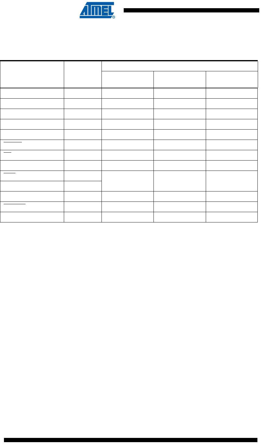
Table 5-2. Address Space
Paging Decodes AT17F16 (16 Mbits)
PAGESEL = 00, PAGE_EN = 1 00000 – 3FFFFh
PAGESEL = 01, PAGE_EN = 1 40000 – 7FFFFh
PAGESEL = 10, PAGE_EN = 1 80000 – BFFFFh
PAGESEL = 11, PAGE_EN = 1 C0000 – FFFFFh
PAGESEL = XX, PAGE_EN = 0 00000 – FFFFFh