TC7106/A/TC7107/A
DS21455D-page 4 © 2008 Microchip Technology Inc.
1.0 ELECTRICAL
CHARACTERISTICS
Absolute Maximum Ratings†
TC7106A
Supply Voltage (V+ to V-)..................................................15V
Analog Input Voltage (either Input) (Note 1) .............. V+ to V-
Reference Input Voltage (either Input) ....................... V+ to V-
Clock Input ..............................................................Test to V+
Package Power Dissipation (T
A
≤ 70°C) (Note 2):
40-Pin PDIP......................................................1.23W
44-Pin PLCC.....................................................1.23W
44-Pin MQFP....................................................1.00W
Operating Temperature Range:
C (Commercial) Devices........................0°C to +70°C
I (Industrial) Devices..........................-25°C to +85°C
Storage Temperature Range.........................-65°C to +150°C
TC7107A
Supply Voltage (V+)..........................................................+6V
Supply Voltage (V-)............................................................-9V
Analog Input Voltage (either Input) (Note 1).............. V+ to V-
Reference Input Voltage (either Input)....................... V+ to V-
Clock Input.............................................................GND to V+
Package Power Dissipation (T
A
≤ 70°C) (Note 2):
40-Pin PDIP......................................................1.23W
44-Pin PLCC ....................................................1.23W
44-Pin MQFP....................................................1.00W
Operating Temperature Range:
C (Commercial) Devices ....................... 0°C to +70°C
I (Industrial) Devices..........................-25°C to +85°C
Storage Temperature Range.........................-65°C to +150°C
† Notice: Stresses above those listed under “Absolute Maximum
Ratings” may cause permanent damage to the device. These are
stress ratings only and functional operation of the device at these or
any other conditions above those indicated in the operation sections of
the specifications is not implied. Exposure to Absolute Maximum Rat-
ing conditions for extended periods may affect device reliability.
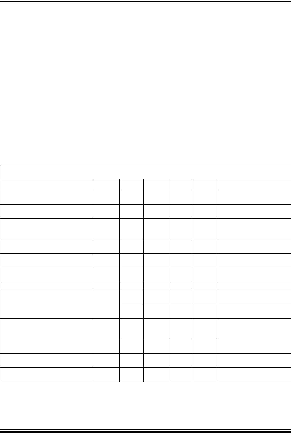
TC7106/A AND TC7107/A ELECTRICAL SPECIFICATIONS
Electrical Characteristics: Unless otherwise noted, specifications apply to both the TC7106/TC7106A and TC7107/TC7107A at
T
A
= +25°C, f
CLOCK
= 48 kHz. Parts are tested in the circuit of the Typical Operating Circuit.
Parameter Symbol Min Typ Max Unit Test Conditions
Zero Input Reading Z
IR
-000.0 ±000.0 +000.0 Digital
Reading
V
IN
= 0.0V
Full Scale = 200.0 mV
Ratiometric Reading 999 999/1000 1000 Digital
Reading
V
IN
= V
REF
V
REF
= 100 mV
Rollover Error (Difference in Reading for
Equal Positive and Negative Reading
Near Full Scale)
R/O -1 ±0.2 +1 Counts V
IN
- = + V
IN
+ ≅ 200 mV
Linearity (Maximum Deviation from Best
Straight Line Fit)
-1 ±0.2 +1 Counts Full Scale = 200 mV or
Full Scale = 2.000V
Common Mode Rejection Ratio (Note 3) CMRR — 50 — µV/V V
CM
= ±1V, V
IN
= 0V,
Full Scale = 200.0 mV
Noise (Peak to Peak Value not
Exceeded 95% of Time)
e
N
—15—µVV
IN
= 0V
Full Scale - 200.0 mV
Leakage Current at Input I
L
— 1 10 pA V
IN
= 0V
Zero Reading Drift — 0.2 1 µV/°C V
IN
= 0V
“C” Device = 0°C to +70°C
—1.0 2µV/°CV
IN
= 0V
“I” Device = -25°C to +85°C
Scale Factor Temperature Coefficient TC
SF
— 1 5 ppm/°C V
IN
= 199.0 mV,
“C” Device = 0°C to +70°C (Ext.
Ref = 0 ppm°C)
— — 20 ppm/°C V
IN
= 199.0 mV
“I” Device = -25°C to +85°C
Supply Current (Does not include LED
Current For TC7107/A)
I
DD
—0.81.8mAV
IN
= 0.8
Analog Common Voltage (with Respect
to Positive Supply)
V
C
2.7 3.05 3.35 V 25 kΩ Between Common and
Positive Supply
Note 1: Input voltages may exceed the supply voltages, provided the input current is limited to ±100 µA.
2: Dissipation rating assumes device is mounted with all leads soldered to printed circuit board.
3: Refer to “Differential Input” discussion.
4: Backplane drive is in phase with segment drive for “OFF” segment, 180° out of phase for “ON” segment. Frequency is 20
times the conversion rate. Average DC component is less than 50 mV.

