ILD1, ILD2, ILD5, ILQ1, ILQ2, ILQ5
www.vishay.com
Vishay Semiconductors
Rev. 1.8, 28-Jun-11
1
Document Number: 83646
For technical questions, contact: optocoupleranswers@vishay.com
THIS DOCUMENT IS SUBJECT TO CHANGE WITHOUT NOTICE. THE PRODUCTS DESCRIBED HEREIN AND THIS DOCUMENT
ARE SUBJECT TO SPECIFIC DISCLAIMERS, SET FORTH AT www.vishay.com/doc?91000
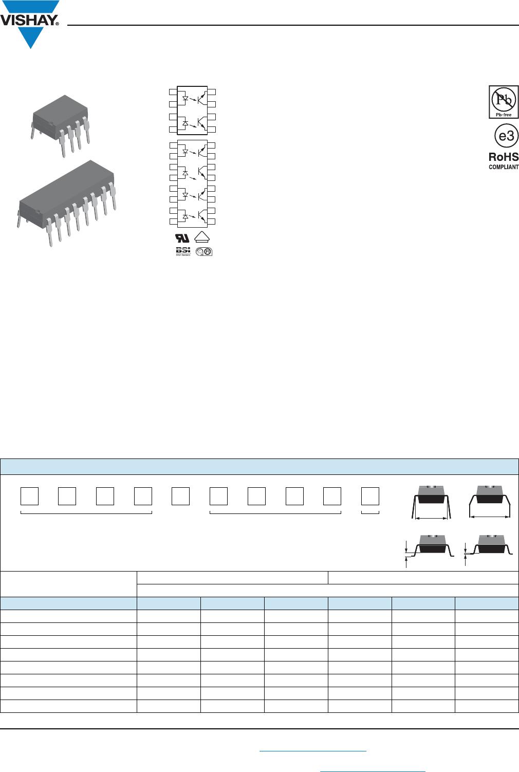
Optocoupler, Phototransistor Output (Dual, Quad Channel)
DESCRIPTION
The ILD1, ILD2, ILD5, ILQ1, ILQ2, ILQ5 are optically coupled
isolated pairs employing GaAs infrared LEDs and silicon
NPN phototransistor. Signal information, including a DC
level, can be transmitted by the drive while maintaining a
high degree of electrical isolation between input and output.
The ILD1, ILD2, ILD5, ILQ1, ILQ2, ILQ5 are especially
designed for driving medium-speed logic and can be used
to eliminate troublesome ground loop and noise problems.
Also these couplers can be used to replace relays and
transformers in many digital interface applications such as
CTR modulation.
The ILD1, ILD2, ILD5 has two isolated channels in a single
DIP package and the ILQ1, ILQ2, ILQ5 has four isolated
channels per package.
FEATURES
Current transfer ratio at I
F
= 10 mA
Isolation test voltage, 5300 V
RMS
Compliant to RoHS Directive 2002/95/EC and
in accordance to WEEE 2002/96/EC
AGENCY APPROVALS
UL1577, file no. E52744 system code H, double protection
CSA 93751
BSI IEC 60950; IEC 60065
DIN EN 60747-5-2 (VDE 0884) available with option 1
•FIMKO
i179015-3
1
2
3
4
8
7
6
5
E
C
C
E
A
C
C
A
A
C
C
A
A
C
C
A
E
C
C
E
E
C
C
E
16
15
14
13
12
11
10
9
1
2
3
4
5
6
7
8
V
DE
i179012-1
Dual Channel
Quad Channel
ORDERING INFORMATION
ILx#-X0##T
PART NUMBER
x = D (Dual) or Q (Quad)
PACKAGE OPTION TAPE AND
REEL
AGENCY CERTIFIED/PACKAGE
DUAL CHANNEL QUAD CHANNEL
CTR (%)
UL, CSA, BSI, FIMKO 20 to 300 100 to 500 50 to 400 20 to 300 100 to 500 50 to 400
DIP-8 ILD1 ILD2 ILD5 - - -
DIP-8, 400 mil, option 6 - ILD2-X006 - - - -
SMD-8, option 7 ILD1-X007T
(1)
ILD2-X007T
(1)
----
SMD-8, option 9 ILD1-X009T
(1)
ILD2-X009T
(1)
ILD5-X009T
(1)
---
DIP-16 - - - ILQ1 ILQ2 ILQ5
DIP-16, 400 mil, option 6 - - - ILQ1-X006 ILQ2-X006 -
SMD-16, option 7 - - - ILQ1-X007 ILQ2-X007T
(1)
-
SMD-16, option 9 - - - ILQ1-X009T
(1)
ILQ2-X009T
(1)
ILQ5-X009T
(1)
> 0.1 mm
10.16 mm
> 0.7 mm
7.62 mm
DIP-#
Option 7
Option 6
Option 9
ILD1, ILD2, ILD5, ILQ1, ILQ2, ILQ5
www.vishay.com
Vishay Semiconductors
Rev. 1.8, 28-Jun-11
2
Document Number: 83646
For technical questions, contact: optocoupleranswers@vishay.com
THIS DOCUMENT IS SUBJECT TO CHANGE WITHOUT NOTICE. THE PRODUCTS DESCRIBED HEREIN AND THIS DOCUMENT
ARE SUBJECT TO SPECIFIC DISCLAIMERS, SET FORTH AT www.vishay.com/doc?91000
Notes
Additional options may be possible, please contact sales office.
(1)
Also available in tubes; do not put T on end.
Notes
Stresses in excess of the absolute maximum ratings can cause permanent damage to the device. Functional operation of the device is not
implied at these or any other conditions in excess of those given in the operational sections of this document. Exposure to absolute
maximum ratings for extended periods of the time can adversely affect reliability.
(1)
Refer to reflow profile for soldering conditions for surface mounted devices (SMD). Refer to wave profile for soldering conditions for throught
hole devices (DIP).
VDE, UL, CSA, BSI, FIMKO 20 to 300 100 to 500 50 to 400 20 to 300 100 to 500 50 to 400
DIP-8 ILD1-X001 ILD2-X001 ILD5-X001 - - -
DIP-8, 400 mil, option 6 - ILD2-X016 - - - -
SMD-8, option 7 - ILD2-X017 - - - -
SMD-8, option 9 ILD1-X019T - - - - -
DIP-16 - - - - ILQ2-X001 -
DIP-16, 400 mil, option 6 - - - - ILQ2-X016 -
SMD-16, option 7 - - - - ILQ2-X017T
(1)
-
ABSOLUTE MAXIMUM RATINGS (T
amb
= 25 °C, unless otherwise specified)
PARAMETER TEST CONDITION PART SYMBOL VALUE UNIT
INPUT
Reverse voltage V
R
6V
Forward current I
F
60 mA
Surge current I
FSM
2.5 A
Power dissipation P
diss
100 mW
Derate linearly from 25 °C 1.3 mW/°C
OUTPUT
Collector emitter reverse voltage
ILD1 V
CEO
50 V
ILQ1 V
CEO
50 V
ILD2 V
CEO
70 V
ILQ2 V
CEO
70 V
ILD5 V
CEO
70 V
ILQ5 V
CEO
70 V
Collector current
I
C
50 mA
t < 1 ms I
C
400 mA
Power dissipation P
diss
200 mW
Derate lineary from 25 °C 2.6 mW/°C
COUPLER
Isolation test voltage
between emitter and detector
V
ISO
5300 V
RMS
Creepage distance 7mm
Clearance distance 7mm
Isolation resistance
V
IO
= 500 V, T
amb
= 25 °C R
IO
10
12
V
IO
= 500 V, T
amb
= 100 °C R
IO
10
11
Package power dissipation P
tot
250 mW
Derate linearly from 25 °C 3.3 mW/°C
Storage temperature T
stg
- 40 to + 150 °C
Operating temperature T
amb
- 40 to + 100 °C
Junction temperature T
j
100 °C
Soldering temperature
(2)
2 mm from case bottom T
sld
260 °C
AGENCY CERTIFIED/PACKAGE
DUAL CHANNEL QUAD CHANNEL
CTR (%)
ILD1, ILD2, ILD5, ILQ1, ILQ2, ILQ5
www.vishay.com
Vishay Semiconductors
Rev. 1.8, 28-Jun-11
3
Document Number: 83646
For technical questions, contact: optocoupleranswers@vishay.com
THIS DOCUMENT IS SUBJECT TO CHANGE WITHOUT NOTICE. THE PRODUCTS DESCRIBED HEREIN AND THIS DOCUMENT
ARE SUBJECT TO SPECIFIC DISCLAIMERS, SET FORTH AT www.vishay.com/doc?91000
Note
Minimum and maximum values are testing requirements. Typical values are characteristics of the device and are the result of engineering
evaluation. Typical values are for information only and are not part of the testing requirements.
ELECTRICAL CHARACTERISTICS (T
amb
= 25 °C, unless otherwise specified)
PARAMETER TEST CONDITION SYMBOL MIN. TYP. MAX. UNIT
INPUT
Forward voltage I
F
= 60 mA V
F
1.25 1.65 V
Reverse current V
R
= 6 V I
R
0.01 10 μA
Capacitance V
R
= 0 V, f = 1 MHz C
O
25 pF
Thermal resistance, junction to lead T
thJL
750 K/W
OUTPUT
Collector emitter capacitance V
CE
= 5 V, f = 1 MHz C
CE
6.8 pF
Collector emitter leakage current V
VCE
= 10 V I
CEO
550nA
Saturation voltage, collector emitter I
C
= 1 mA, I
B
= 20 μA V
CESAT
0.25 0.4 V
DC forward current gain V
CE
= 10 V, I
B
= 20 μA h
FE
200 650 1800
DC forward current gain saturated V
CE
= 0.4 V, I
B
= 20 μA h
FEsat
120 400 600
Thermal resistance, junction to lead R
thjl
500 K/W
COUPLER
Capacitance (input to output) V
IO
= 0 V, f = 1 MHz C
IO
0.8 pF
CURRENT TRANSFER RATIO (T
amb
= 25 °C, unless otherwise specified)
PARAMETER TEST CONDITION PART SYMBOL MIN. TYP. MAX. UNIT
I
C
/I
F
(collector emitter
saturated)
I
F
=10 mA, V
CE
= 0.4 V
ILD1 CTR
CEsat
75 %
ILQ1 CTR
CEsat
75 %
ILD2 CTR
CEsat
170 %
ILQ2 CTR
CEsat
170 %
ILD5 CTR
CEsat
100 %
ILQ5 CTR
CEsat
100 %
I
F
=10 mA, V
CE
= 10 V
ILD1 CTR
CE
20 80 300 %
ILQ1 CTR
CE
20 80 300 %
ILD2 CTR
CE
100 200 500 %
ILQ2 CTR
CE
100 200 500 %
ILD5 CTR
CE
50 130 400 %
ILQ5 CTR
CE
50 130 400 %

ILD5-X009T

Mfr. #:
Manufacturer:
Vishay Semiconductors
Description:
Transistor Output Optocouplers Phototransistor Out Dual CTR > 50%
Lifecycle:
New from this manufacturer.
Delivery:
DHL FedEx Ups TNT EMS
Payment:
T/T Paypal Visa MoneyGram Western Union