NUD3105DMT1G

© Semiconductor Components Industries, LLC, 2009
October, 2009 Rev. 5
1 Publication Order Number:
NUD3105D/D
NUD3105D
Integrated Relay,
Inductive Load Driver
This device is used to switch inductive loads such as relays,
solenoids incandescent lamps, and small DC motors without the need
of a freewheeling diode. The device integrates all necessary items
such as the MOSFET switch, ESD protection, and Zener clamps. It
accepts logic level inputs thus allowing it to be driven by a large
variety of devices including logic gates, inverters, and
microcontrollers.
Features
Provides a Robust Driver Interface Between D.C. Relay Coil and
Sensitive Logic Circuits
Optimized to Switch Relays from 3.0 V to 5.0 V Rail
Capable of Driving Relay Coils Rated up to 2.5 W at 5.0 V
Internal Zener Eliminates the Need of FreeWheeling Diode
Internal Zener Clamp Routes Induced Current to Ground for Quieter
Systems Operation
Low V
DS(on)
Reduces System Current Drain
PbFree Package is Available
Typical Applications
Telecom: Line Cards, Modems, Answering Machines, FAX
Computers and Office: Photocopiers, Printers, Desktop Computers
Consumer: TVs and VCRs, Stereo Receivers, CD Players,
Cassette Recorders
Industrial: Small Appliances, Security Systems, Automated Test
Equipment, Garage Door Openers
Automotive: 5.0 V Driven Relays, Motor Controls, Power Latches,
Lamp Drivers
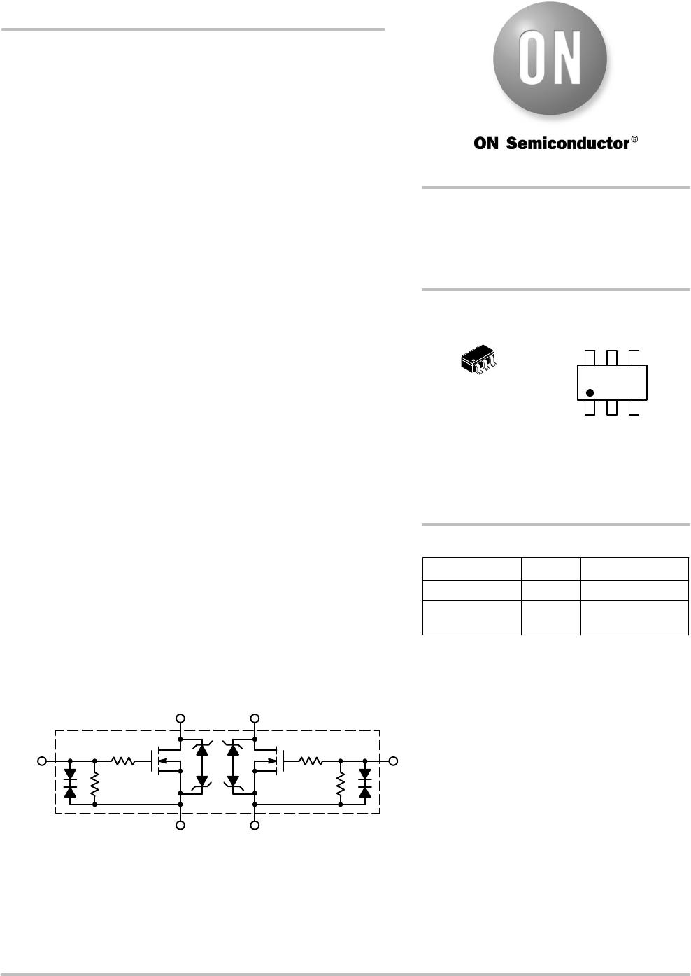
INTERNAL CIRCUIT DIAGRAMS
Drain (6)
1.0 k
300 k
Gate (2)
Source (1)
Drain (3)
1.0 k
300 k
Gate (5)
Source (4)
CASE 318F
Device Package Shipping
ORDERING INFORMATION
MARKING
DIAGRAM
Relay, Inductive Load Driver
0.5 Amp, 8.0 V Clamp
NUD3105DMT1 SC74 3000/Tape & Reel
SC74
CASE 318F
STYLE 7
JW4 = Specific Device Code
D = Date Code
G = PbFree Package
JW4 D G
G
For information on tape and reel specifications,
including part orientation and tape sizes, please
refer to our Tape and Reel Packaging Specification
Brochure, BRD8011/D.
(Note: Microdot may be in either location)
http://onsemi.com
NUD3105DMT1G
SC74
(PbFree)
3000/Tape & Reel
1
6
NUD3105D
http://onsemi.com
2
MAXIMUM RATINGS (T
J
= 25°C unless otherwise specified)
Symbol Rating Value Unit
V
DSS
Drain to Source Voltage Continuous 6.0 V
dc
V
GS
Gate to Source Voltage – Continuous 6.0 V
dc
I
D
Drain Current – Continuous 500 mA
E
z
Single Pulse DraintoSource Avalanche Energy (T
Jinitial
=
25°C)
50 mJ
T
J
Junction Temperature 150 °C
T
A
Operating Ambient Temperature 40 to 85 °C
T
stg
Storage Temperature Range 65 to +150 °C
P
D
Total Power Dissipation (Note 1)
Derating Above 25°C
380
1.5
mW
mW/°C
R
q
JA
Thermal Resistance JunctiontoAmbient 329 °C/W
Stresses exceeding Maximum Ratings may damage the device. Maximum Ratings are stress ratings only. Functional operation above the
Recommended Operating Conditions is not implied. Extended exposure to stresses above the Recommended Operating Conditions may affect
device reliability.
1. This device contains ESD protection and exceeds the following tests:
Human Body Model 2000 V per MIL_STD883, Method 3015.
Machine Model Method 200 V.
TYPICAL ELECTRICAL CHARACTERISTICS (T
J
= 25°C unless otherwise noted)
Symbol Characteristic Min Typ Max Unit
OFF CHARACTERISTICS
V
BRDSS
Drain to Source Sustaining Voltage (Internally Clamped)
(I
D
= 10 mA)
6.0 8.0 9.0 V
B
VGSO
I
g
= 1.0 mA 8.0 V
I
DSS
Drain to Source Leakage Current
(V
DS
= 5.5 V , V
GS
= 0 V, T
J
= 25°C)
(V
DS
= 5.5 V, V
GS
= 0 V, T
J
= 85°C )
15
15
mA
I
GSS
Gate Body Leakage Current
(V
GS
= 3.0 V, V
DS
= 0 V)
(V
GS
= 5.0 V, V
DS
= 0 V)
5.0
35
65
mA
ON CHARACTERISTICS
V
GS(th)
Gate Threshold Voltage
(V
GS
= V
DS
, I
D
= 1.0 mA)
(V
GS
= V
DS
, I
D
= 1.0 mA, T
J
= 85°C)
0.8
0.8
1.2
1.4
1.4
V
R
DS(on)
Drain to Source OnResistance
(I
D
= 250 mA, V
GS
= 3.0 V)
(I
D
= 500 mA, V
GS
= 3.0 V)
(I
D
= 500 mA, V
GS
= 5.0 V)
(I
D
= 500 mA, V
GS
= 3.0 V, T
J
= 85°C)
(I
D
= 500 mA, V
GS
= 5.0 V, T
J
= 85°C)
1.2
1.3
0.9
1.3
0.9
W
I
DS(on)
Output Continuous Current
(V
DS
= 0.25 V, V
GS
= 3.0 V)
(V
DS
= 0.25 V, V
GS
= 3.0 V, T
J
= 85°C)
300
200
400
mA
g
FS
Forward Transconductance
(V
OUT
= 5.0 V, I
OUT
= 0.25 A)
350 570 mMhos
NUD3105D
http://onsemi.com
3
TYPICAL ELECTRICAL CHARACTERISTICS (T
J
= 25°C unless otherwise noted)
Symbol UnitMaxTypMinCharacteristic
DYNAMIC CHARACTERISTICS
C
iss
Input Capacitance
(V
DS
= 5.0 V,V
GS
= 0 V, f = 10 kHz)
25 pF
C
oss
Output Capacitance
(V
DS
= 5.0 V, V
GS
= 0 V, f = 10 kHz)
37 pF
C
rss
Transfer Capacitance
(V
DS
= 5.0 V, V
GS
= 0 V, f = 10 kHz)
8.0 pF
SWITCHING CHARACTERISTICS
Symbol Characteristic Min Typ Max Units
t
PHL
t
PLH
t
PHL
t
PLH
Propagation Delay Times:
High to Low Propagation Delay; Figure 1 (5.0 V)
Low to High Propagation Delay; Figure 1 (5.0 V)
High to Low Propagation Delay; Figure 1 (3.0 V)
Low to High Propagation Delay; Figure 1 (3.0 V)
25
80
44
44
nS
t
f
t
r
t
f
t
r
Transition Times:
Fall Time; Figure 1 (5.0 V)
Rise Time; Figure 1 (5.0 V)
Fall Time; Figure 1 (3.0 V)
Rise Time; Figure 1 (3.0 V)
23
32
53
30
nS
Figure 1. Switching Waveforms
V
out
GND
V
in
GND
V
Z
V
CC
V
CC
t
r
t
f
t
PLH
t
PHL
50%
90%
50%
10%

NUD3105DMT1G

Mfr. #:
Manufacturer:
ON Semiconductor
Description:
Gate Drivers 5V Dual Integrated Relay Inductive Load
Lifecycle:
New from this manufacturer.
Delivery:
DHL FedEx Ups TNT EMS
Payment:
T/T Paypal Visa MoneyGram Western Union

Products related to this Datasheet