Expand menu
Hello, Sign in
My Account
0
Cart
Home
Products
Sensors
Semiconductors
Passive Components
Connectors
Power
Electromechanical
Optoelectronics
Circuit Protection
Integrated Circuits - ICs
Main Products
Manufacturers
Blog
Services
About OMO
About Us
Contact Us
Check Stock
ZL40204LDF1
P1-P3
P4-P6
P7-P9
P10-P12
P13-P15
P16-P18
P19-P21
P22-P24
P25-P26
VDD
2 K
Ohm
VDD_dri
ver
VDD
ZL40204
clk_p
clk_n
Z
o
= 50 Ohms
Z
o
= 50 Ohms
2 K
Ohm
2 K
Ohm
2 K
Ohm
CML
Drive
r
100 nF
100 nF
VDD_driver
50
Ohm
50
Ohm
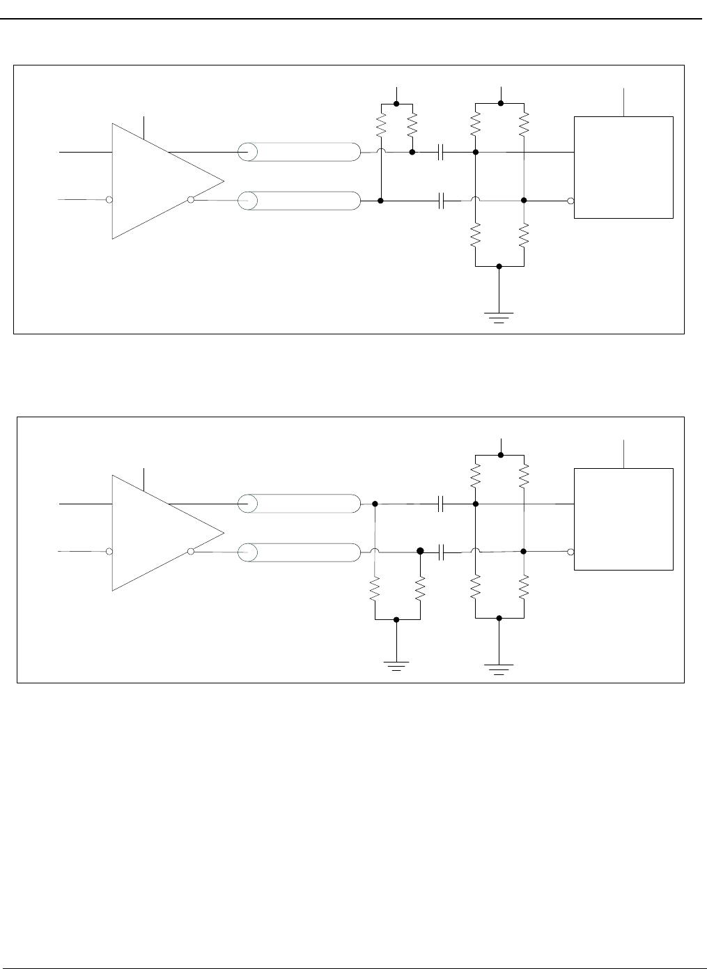
Figure 8 - CM
L Input AC Coupled
VDD
2 K
Ohm
VDD_dri
ver
VDD
ZL40204
clk_p
clk_n
Z
o
= 50 Ohms
Z
o
= 50 Ohms
2 K
Ohm
2 K
Ohm
2 K
Ohm
HCSL
Drive
r
100 nF
100 nF
50
Ohm
50
Ohm
Figure 9 - HCSL Input AC Coupled
ZL40204
Data Sheet
9
Microsemi Corporation
VDD_driver
VDD_driver
VDD
ZL40204
clk_p
clk_n
CMOS
Driver
R
R
C
Vref = VDD_driver/2
For VDD_Driver = 2.5 or 3.3 V onl
y
R=10
k oh
m
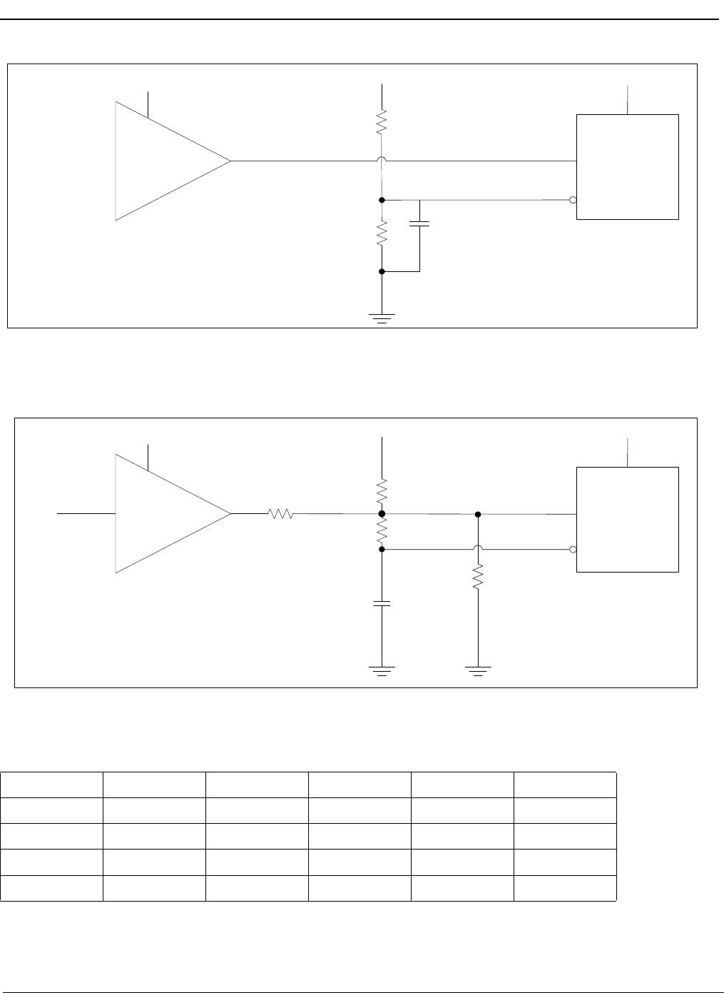
Figure 10 - CMOS Input DC Coupled Referenced to VDD/2
VDD
VDD_driver
VDD
ZL40204
clk_p
clk_n
CMOS
Driver
R2
C
RA
R3
R1
Figure 1
1 - CMOS Input DC Coupled Referenced to Grou
nd
T
able 1 - Component V
alues for Single Ended Input Reference to Grou
nd
VDD_driver
R1 (k
Ω
)
R2 (k
Ω
)
R3 (k
Ω
)
RA (k
Ω
)
C (pF)
1.5
1.25
3.075
open
10
10
1.8
1
3.8
open
10
10
2.5
0.33
4.2
open
10
10
3.3
0.75
open
4.2
10
10
ZL40204
Data Sheet
10
Microsemi Corporation
* For frequencies below 100 MHz, incr
ease
C to avoid signal integrity issues.
ZL40204
Data Sheet
11
Microsemi Corporation
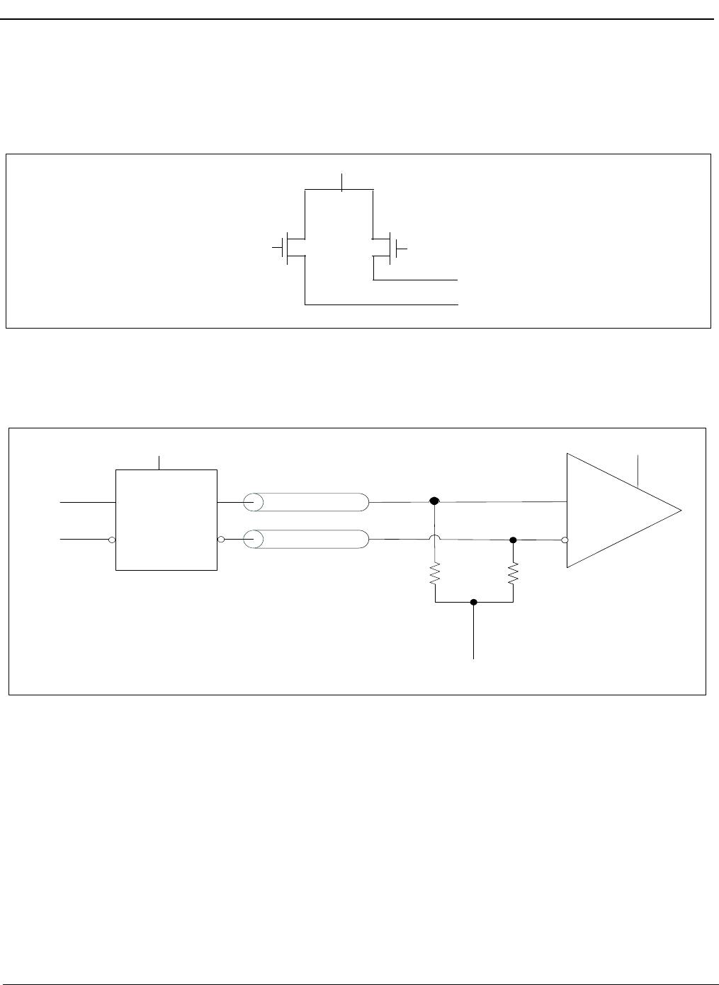
3.2 Clock Output
s
L
VPECL has a very low output impedance and a differential signal swing between 1V and 1.6
V
. A simplified
diagram for the output stage is shown in Figure 12
.The L
VPECL to L
VDS output termination is not shown since
there is a separate device that has the same input and L
VDS outputs.
Figure 12 - Simplified Output Driver
out_p
out_n
The methods to terminate the ZL40204 L
VPECL dr
ivers are shown in the following figures.
LVP
E
CL
Rece
i
ver
50
Ohms
50
Ohms
VDD
VDD_
Rx
Z
o
= 50 Ohm
s
Z
o
= 50 Ohm
s
ZL40204
cl
k_p
cl
k_n
VDD -
2
Figure 13 - L
VPEC
L Basic Output T
ermination
P1-P3
P4-P6
P7-P9
P10-P12
P13-P15
P16-P18
P19-P21
P22-P24
P25-P26
ZL40204LDF1
Mfr. #:
Buy ZL40204LDF1
Manufacturer:
Microchip / Microsemi
Description:
Clock Buffer 1:6 LVPECL Fanout Buffer w/Ext. Term.
Lifecycle:
New from this manufacturer.
Delivery:
DHL
FedEx
Ups
TNT
EMS
Payment:
T/T
Paypal
Visa
MoneyGram
Western
Union
Products related to this Datasheet
ZL40204LDG1
ZL40204LDF1