ZL40204 Data Sheet
15
Microsemi Corporation
3.3 Device Additive Jitter
The ZL40204 clock fan out buffer is not intended to filter clock jitter. The jitter performance of this type of device is
characterized by its additive jitter. Additive jitter is the jitter the device would add to a hypothetical jitter-free clock as
it passes through the device. The additive jitter of the ZL40204 is random and as such it is not correlated to the jitter
of the input clock signal.
The square of the resultant random RMS jitter at the output
of the ZL40204 is equal to the sum of the squares of the
various random RMS jitter sources including: input clock jitter; additive jitter of the buffer; and additive jitter due to
power supply noise. There may be additional deterministic jitter sources that are not shown in Figure 19.
+
J
in
2
J
out
2
= J
in
2
+J
add
2
+J
ps
2
J
add
2
J
ps
2
J
in
= Random input clock jitter (RMS)
J
add
= Additive jitter due to the device (RMS)
J
ps
= Additive jitter due to power supply noise (RMS)
J
out
= Resultant random output clock jitter (RMS)
+
Figure 19 - Additive Jitter
ZL40204 Data Sheet
16
Microsemi Corporation
3.4 Power Supply
This device operates employing either a 2.5V supply or 3.3V supply.
3.4.1 Sensitivity to power supply noise
Power supply noise from sources such as switching power supplies and high-power digital components such as
FPGAs can induce additive jitter on clock buffer outputs. The ZL40204 is equipped with a low drop out (LDO) on-
chip linear power regulator and on-chip bulk capacitors to minimize additive jitter due to power supply noise. The
on-chip regulation, recommended power supply filtering, and good PCB layout all work together to minimize the
additive jitter from power supply noise.
3.4.2 Power supply filtering
Jitter levels may increase when noise is present on the power pins. For optimal jitter performance, the device
should be isolated from the power planes connected to its power supply pins as shown in Figure 20.
ZL40204
1
8
9
19
22
32
0.1 µF
0.1 µF
vdd_core
10 µF
0.1 µF
0.15
vdd
0.1 µF
10 µF
Figure 20 - Decoupling Connections for Power Pins
10 µF capacitors should be size 0603 or size 080
5 X5R or X7R ceramic, 6.3 V minimum rating
0.1 µF capacitors should be
size 0402 X5R ceramic, 6.3 V minimum rating
Capacitors should be placed next to the
connected device power pins
A 0.15 ohm resistor is recommended
3.4.3 PCB layout considerations
The power nets in Figure 20 can be implemented either as a plane island or routed power topology without
changing the overall jitter p
erformance of the device.
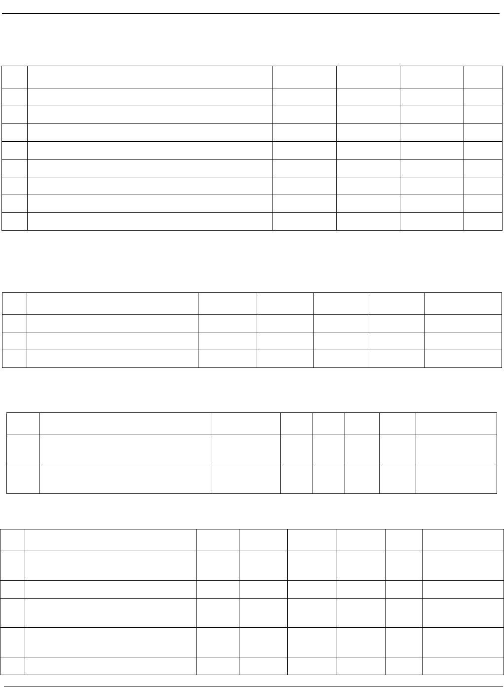
Absolute Maximum Ratings*
Parameter Sym. Min. Max. Units
1 Supply voltage V
DD_R
-0.5 4.6 V
2 Voltage on any digital pin V
PIN
-0.5 V
DD
V
3 LVPECL output current I
out
30 mA
4 Soldering temperature T 260 °C
5 Storage temperature T
ST
-55 125 °C
6 Junction temperature T
j
125 °C
7 Voltage on input pin V
input
V
DD
V
8 Input capacitance each pin C
p
500 fF
ZL40204 Data Sheet
17
Microsemi Corporation
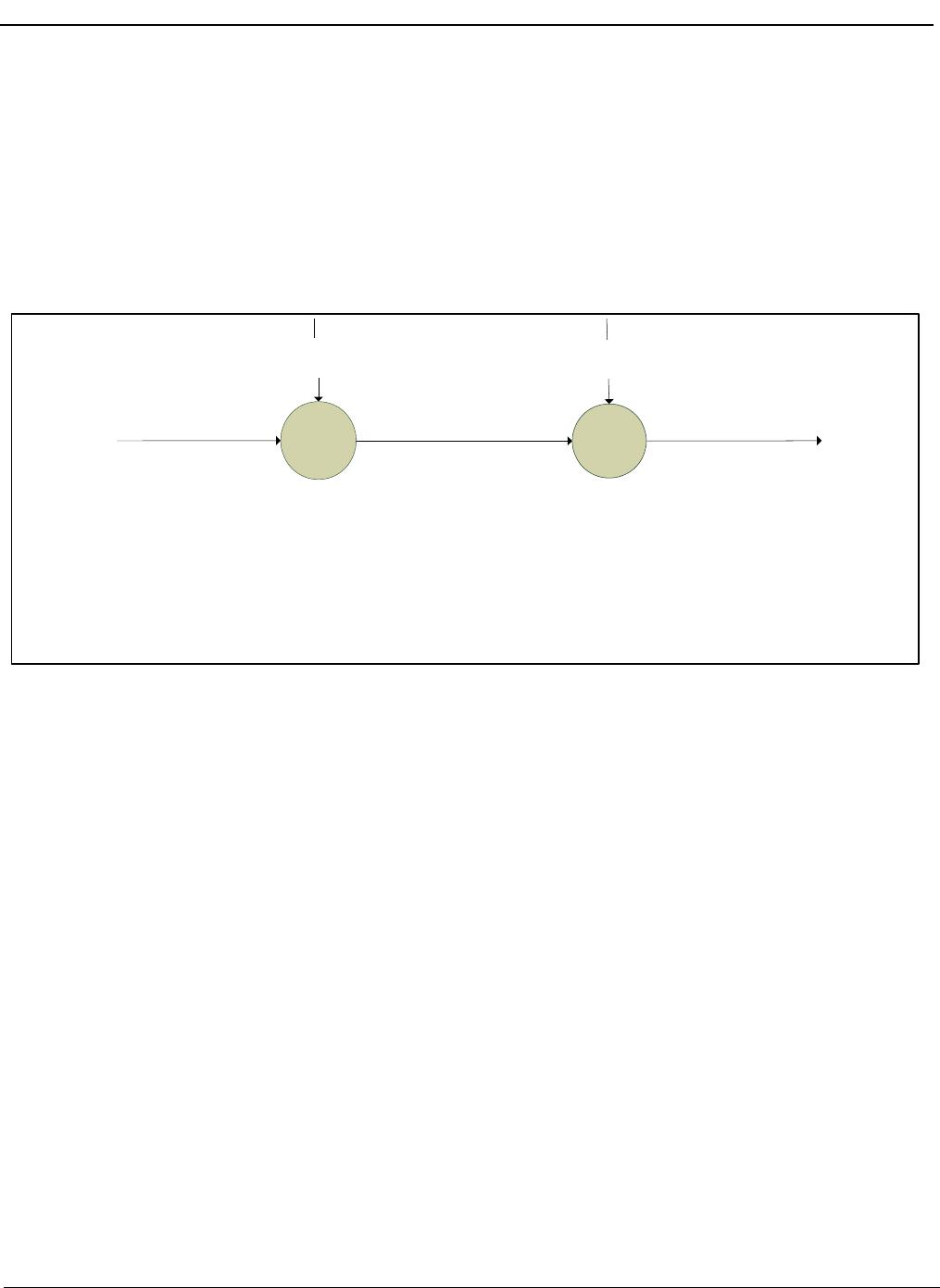
4.0 AC and DC Electrical Characteristics
* Exceeding these values may cause permanent damage. Functional operation under these conditions is not implied.
* Voltages are with respect to ground (GND) unless otherwise stated
Recommended Operating Conditions*
Characteristics Sym. Min. Typ. Max. Units
1 Supply voltage 2.5 V mode V
DD25
2.375 2.5 2.625 V
2 Supply voltage 3.3 V mode V
DD33
3.135 3.3 3.465 V
3 Operating temperature T
A
-40 25 85 °C
* Voltages are with respect to ground (GND) unless otherwise stated
DC Electrical Characteristics - Current Consumption
Characteristics Sym. Min. Typ. Max. Units Notes
1 Supply current LVPECL drivers -
un
loaded
I
dd_unload
110 mA
2
Supply current LVPECL drivers -
loa
ded (all outputs are active)
I
dd_load
209 mA Including power
to R
L
= 50Ω
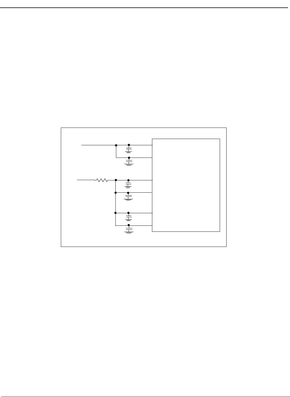
DC Electrical Characteristics - Input
s and Outputs - for 3.3 V Supply
Characteristics Sym. Min. Typ. Max. Units Notes
1 Differential input com
mon mode
voltage
V
CM
1.1 2.0 V
2 Differential input volt
age difference V
ID
0.25 1 V
3 LVPECL output high voltage V
OH
V
DD
-
1.4
V
4 LVPECL output low voltage V
OL
V
DD
-
1.62
V
5 LVPECL output differential voltage* V
OD
0.5 0.9 V

ZL40204LDF1

Mfr. #:
Manufacturer:
Microchip / Microsemi
Description:
Clock Buffer 1:6 LVPECL Fanout Buffer w/Ext. Term.
Lifecycle:
New from this manufacturer.
Delivery:
DHL FedEx Ups TNT EMS
Payment:
T/T Paypal Visa MoneyGram Western Union

Products related to this Datasheet