HMC8038 Data Sheet
Rev. A | Page 6 of 11
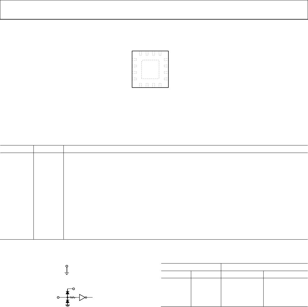
PIN CONFIGURATION AND FUNCTION DESCRIPTIONS
12
11
10
1
3
4
9
2
6
5
7
8
16
15
14
13
V
DD
V
CTL
RFC
NC
RF2
NC
NC
NC
NC
GND
GND
RF1
EN
NC
NC
NC
HMC8038
TOP VIEW
(Not to Scale)
NOTES
1. NC = NO CONNECT. THE PINS ARE NOT CONNECTED
INTERNALLY; HOWEVER, ALL DATA SHOWN HEREIN WAS
MEASURED WITH THESE PINS CONNECTED TO RF/DC
GROUND EXTERNALLY.
2. EXPOSED PAD. EXPOSED PAD MUST BE CONNECTED TO
RF/DC GROUND.
13554-003
Figure 3. Pin Configuration
Table 5. Pin Function Descriptions
Pin No. Mnemonic Description
1 V
DD
Supply Voltage Pin.
2 V
CTL
Control Input Pin. See Figure 5 for the V
CTL
interface schematic. Refer to Table 6 and the recommended input
control voltage range in Table 2.
3 RFC RF Common Port. This pin is dc-coupled and matched to 50 Ω. A dc blocking capacitor is required on this pin.
4, 6 to 8,
13 to 16
NC
Not Internally Connected. These pins are not internally connected; however, all data shown in this data sheet is
measured with the NC pins externally connected to RF/dc ground on the evaluation board.
5 EN
Enable Input Pin. See Figure 5 for the EN interface schematic. Refer to Table 6 and the recommended input
control voltage range in Table 2.
9 RF1 RF Port 1. This pin is dc-coupled and matched to 50 Ω. A dc blocking capacitor is required on this pin.
Ground. The package bottom has an exposed metal pad that must connect to the printed circuit board (PCB)
RF ground. See Figure 4 for the GND interface schematic.
12 RF2 RF Port 2. This pin is dc-coupled and matched to 50 Ω. A dc blocking capacitor is required on this pin.
EPAD Exposed Pad. Exposed pad must be connected to RF/dc ground.
INTERFACE SCHEMATICS
13554-004
Figure 4. GND Interface Schematic
V
DD
V
CTL
, EN
13554-005
Figure 5. Logic Control Interface Schematic
Table 6. Truth Table
Control Input Signal Path State
V
CTL
State EN State RFC to RF1 RFC to RF2
Low Low Off On
High Low On Off
Low High Off Off
High High Off Off