MIC2177 Micrel, Inc.
M9999-031805 2 March 2005
Ordering Information
Part Output Switching Temperature
Number Voltage Frequency Range Package Lead Finish
MIC2177-3.3BWM* 3.3V 200kHz –40°C to +85°C 20-lead WSOP Standard
MIC2177-5.0BWM* 5.0V 200kHz –40°C to +85°C 20-lead WSOP Standard
MIC2177BWM* adj. 200kHz –40°C to +85°C 20-lead WSOP Standard
MIC2177-3.3YWM 3.3V 200kHz –40°C to +85°C 20-lead WSOP Pb-Free
MIC2177-5.0YWM 5.0V 200kHz –40°C to +85°C 20-lead WSOP Pb-Free
MIC2177YWM adj. 200kHz –40°C to +85°C 20-lead WSOP Pb-Free
Pin Description
Pin Number Pin Name Pin Function
1, 2, 9 VIN Supply Input: Controller and switch supply. Unregulated supply input to
internal regulator, output switches, and control circuitry. Requires bypass
capacitor to PGND. All three pins must be connected to V
IN
.
3,8 SW Switch (Output): Internal power MOSFET switch output. Both pins must be
externally connected together.
4,5,6,7 PGND Power Ground: Output stage ground connections. Connect all pins to a
common ground plane.
10 OUT Output Voltage Sense (Input): Senses output voltage to determine minimum
switch current for PWM operation. Connect directly to V
OUT
.
11 AUTO Automatic Mode: Connect 2.2nF timing capacitor for automatic PWM-/skip-
mode switching. Regulator operates exclusively in PWM mode when pin is
pulled low.
12 FB Feedback (Input): Error amplifier inverting input. For adjustable output
version, connect FB to external resistive divider to set output voltage. For
3.3V and 5V fixed output versions, connect FB directly to output.
13 COMP Compensation: Internal error amplifier output. Connect to capacitor or series
RC network to compensate the regulator control loop.
14,15,16,17 SGND Signal Ground: Ground connection of control section. Connect all pins to
common ground plane.
18 SYNC Frequency Synchronization (Input): Optional clock input. Connect to
external clock signal to synchronize oscillator. Leading edge of signal above
1.7V terminates switching cycle. Connect to SGND if not used.
19 BIAS Bias Supply: Internal 3.3V bias supply output. Decouple with 0.01µF
bypass capacitor and 10kΩ to SGND. Do not apply any external load.
20 EN Enable (Input): Logic high enables operation. Logic low shuts down
regulator. Do not allow pin to float.
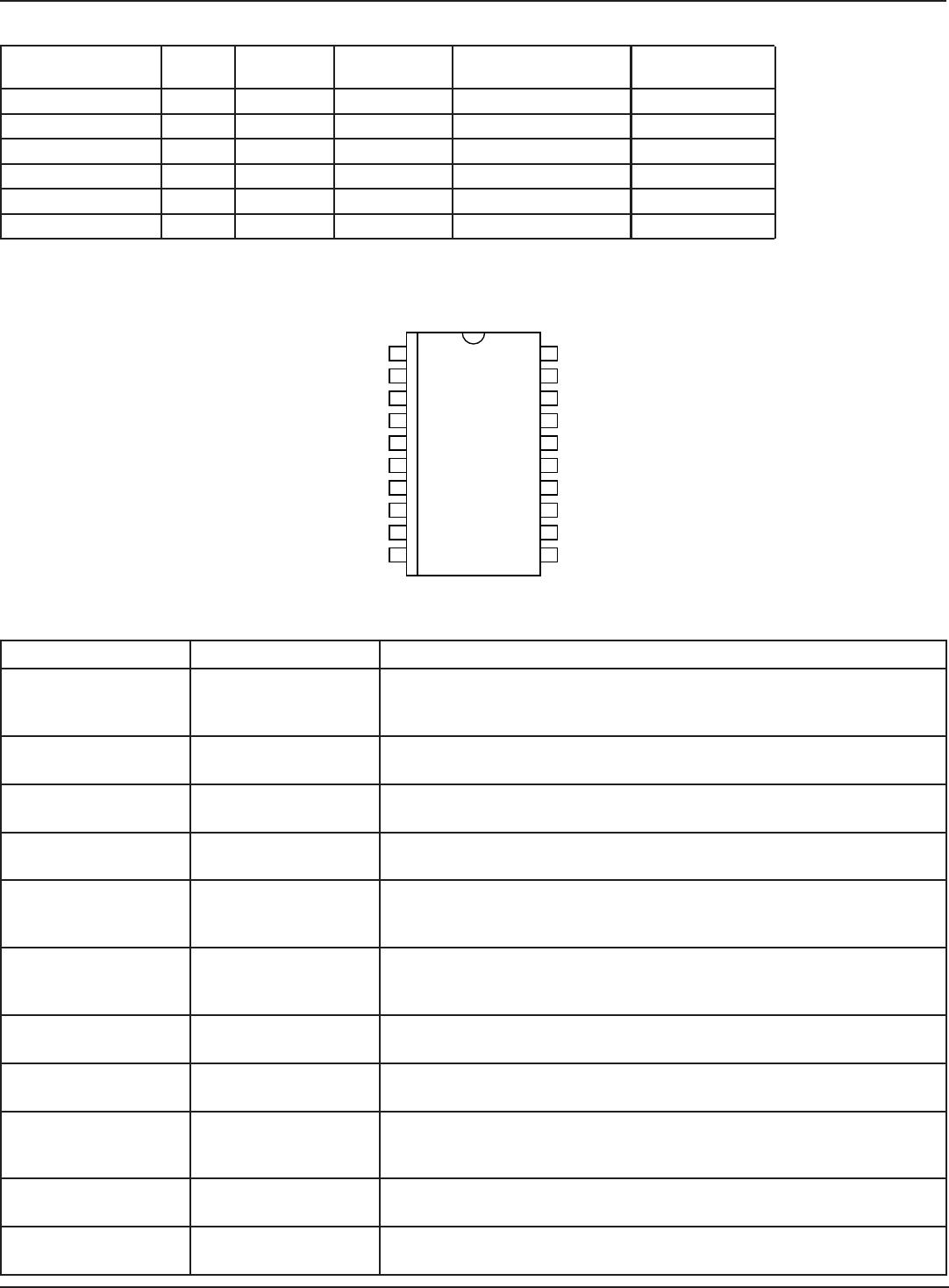
Pin Configuration
2VIN
3SW
4PGND
5PGND
6PGND
7PGND
1VIN
8SW
9
VIN
EN20
BIAS19
SYNC18
SGND17
SGND16
SGND15
10
OUT
14
13
12
11
AUTO
FB
COMP
SGND
20-Lead Wide SOP
* Standard product will be supported as Pb-Free IAW PPCN #040004 effective 1-1-2005 pending residual depletion.,

