March 2005 11 M9999-031805
MIC2177 Micrel, Inc.
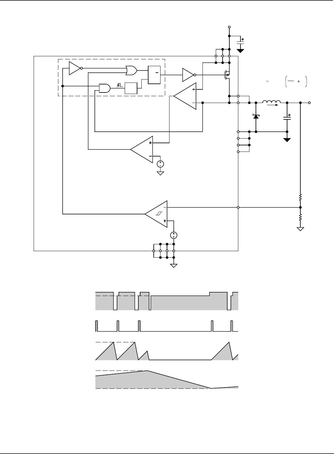
Application Information
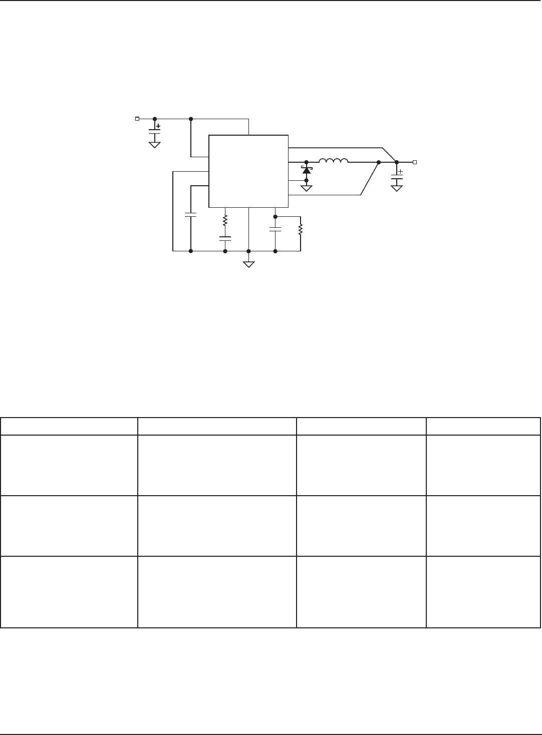
Feedback Resistor Selection (Adjustable Version)
The output voltage is configured by connecting an external
resistive divider to the FB pin as shown in “MIC2177 Block
Diagram.” The ratio of R1 to R2 determines the output
voltage. To optimize efficiency during low output current
operation, R2 should not be less than 20kΩ. However, to
prevent feedback error due to input bias current at the FB pin,
R2 should not be greater than 100kΩ. After selecting R2,
calculate R1 using the following formula:
R1 = R2
V
1.245V
1
OUT
−
Input Capacitor Selection
The input capacitor is selected for its RMS current and
voltage rating and should be a low ESR (equivalent series
resistance) electrolytic or tantalum capacitor. As a rule-of-
thumb, the voltage rating for a tantalum capacitor should be
twice the value of V
IN
, and the voltage rating for an electrolytic
should be 40% higher than V
IN.
The RMS current rating must
be equal or greater than the maximum RMS input ripple
current. A simple, worst-case formula for calculating this
RMS current is:
I =
I
RMS(max)
LOAD(max)
2
Tantalum capacitors are a better choice for applications that
require the most compact layout or operation below 0°C. The
input capacitor must be located very close to the VIN pin
(within 0.2 inches, 5mm). Also place a 0.1µF ceramic bypass
capacitor as close as possible to VIN.
Inductor Selection
The inductor must be at least a minimum value in order for the
MIC2177 to change from PWM to skip mode at the correct
value of output current. This minimum value ensures the
inductor ripple current never exceeds 600mA, and is calcu-
lated using the following formula:
L = V 1 –
V
V
8.3 H/V
MIN
OUT
OUT
IN(max)
×µ
Where:
V
IN(max)
= maximum input voltage
In general, a value at least 20% greater than L
MIN
should be
selected because inductor values have a tolerance of ±20%.
Two other parameters to consider in selecting an inductor are
winding resistance and peak current rating. The inductor
must have a peak current rating equal or greater than the
peak inductor current. Otherwise, the inductor may saturate,
causing excessive current in the output switch. Also, the
inductor’s core loss may increase significantly. Both of these
effects will degrade efficiency. The formula for peak inductor
current is:
I I 300mA
L(peak)
LOAD(max)
=+
To maximize efficiency, the inductor’s resistance must be
less than the output switch on-resistance (preferably 50mΩ
or less).
Output Capacitor Selection
Select an output capacitor that has a low value of ESR. This
parameter determines a regulator’s output ripple voltage
(V
RIPPLE
) which is generated by ∆I
L
× ESR. As mentioned in
“Inductor Selection,” the maximum value for ∆I
L
is 600mA.
Therefore, the maximum value of ESR is:
ESR =
600mA
V
MAX
RIPPLE
Where:
V
RIPPLE
< 1% of V
OUT
Typically, capacitors in the range of 100µF to 220µF have
ESR less than this maximum value. The output capacitor can
be either a low ESR electrolytic or tantalum capacitor, but
tantalum is a better choice for compact layout and operation
at temperatures below 0°C. The voltage rating of a tantalum
capacitor must be 2 × V
OUT
, and the voltage rating of an
electrolytic must be 1.4 × V
OUT
.
Output Diode Selection
In PWM operation, inductor current flows through the output
diode approximately 50ns during the dead time when one
output MOSFET turns off and the other turns on. In skip
mode, the inductor current flows through the diode during the
entire P-channel off time. The correct diode for both of these
conditions is a 1A diode with a reverse voltage rating greater
than V
IN
. It must be a Schottky or ultrafast-recovery diode
(t
R
< 100ns) to minimize power dissipation from the diode’s
reverse-recovery charge.
Compensation
Compensation is provided by connecting a series RC load to
the COMP pin. This creates a pole-zero pair in the regulator
control loop, allowing the regulator to remain stable with
enough low frequency loop-gain for good load and line
regulation. At higher frequencies, pole-zero reduces loop-
gain to a level referred to as the mid-band gain. The mid-band
gain is low enough so that the loop gain crosses 0dB with
sufficient phase margin. Typical values for the RC load are
4.7nF – 10nF for the capacitor and 5kΩ – 20kΩ for the
resistor.
Printed Circuit Board Layout
A well designed PC board will prevent switching noise and
ground bounce from interfering with the operation of the
MIC2177. A good design takes into consideration component
placement and routing of power traces.
The first thing to consider is the locations of the input
capacitor, inductor, output diode, and output capacitor. The
input capacitor must be placed very close to the VIN pin, the
inductor and output diode very close to the SW pin, and the
output capacitor near the inductor. These components pass
large high-frequency current pulses, so they must use short,
wide power traces. In addition, their ground pins and PGND
are connected to a ground plane that is nearest the power
supply ground bus.