13
FN6320.3
April 18, 2007
Example:
V
IN
= 12V
V
O
= 48V
L
s
= 800μH
Ns/Np = 10
Lp = 8.0μH
I
O
= 200mA
Switching Frequency, f
sw
= 200kHz
Duty Cycle, D = 28.6%
R
6
= 499Ω
Solve for the current sense resistor, R
CS
, using Equation 15.
R
CS
= 295mΩ
Determine the amount of voltage, Ve, that must be added to
the current feedback signal using Equation 12.
Ve = 92.4mV
Using Equation 17, solve for the summing resistor, R
9
, from
CT to CS.
R
9
= 2.67kΩ
Determine the new value of R
CS
(R’
CS
) using Equation 18.
R’
CS
= 350mΩ
Additional slope compensation may be considered for
design margin. The above discussion determines the
minimum external ramp that is required. The buffer transistor
used to create the external ramp from RTCT should have a
sufficiently high gain (>200) so as to minimize the required
base current. Whatever base current is required reduces the
charging current into RTCT and will reduce the oscillator
frequency.
Fault Conditions
A Fault condition occurs if VREF falls below 4.65V. When a
Fault is detected OUT is disabled. When VREF exceeds
4.80V, the Fault condition clears, and OUT is enabled.
Ground Plane Requirements
Careful layout is essential for satisfactory operation of the
device. A good ground plane must be employed. A unique
section of the ground plane must be designated for high di/dt
currents associated with the output stage. V
DD
should be
bypassed directly to GND with good high frequency
capacitors.
References
[1] Ridley, R., “A New Continuous-Time Model for Current
Mode Control”, IEEE Transactions on Power
Electronics, Vol. 6, No. 2, April 1991.
ISL8840A, ISL8841A, ISL8842A, ISL8843A, ISL8844A, ISL8845A
14
FN6320.3
April 18, 2007
ISL8840A, ISL8841A, ISL8842A, ISL8843A, ISL8844A, ISL8845A
Small Outline Plastic Packages (SOIC)
INDEX
AREA
E
D
N
123
-B-
0.25(0.010) C AM BS
e
-A-
L
B
M
-C-
A1
A
SEATING PLANE
0.10(0.004)
h x 45°
C
H
0.25(0.010) BM M
α
NOTES:
1. Symbols are defined in the “MO Series Symbol List” in Section 2.2 of
Publication Number 95.
2. Dimensioning and tolerancing per ANSI Y14.5M-1982.
3. Dimension “D” does not include mold flash, protrusions or gate burrs.
Mold flash, protrusion and gate burrs shall not exceed 0.15mm (0.006
inch) per side.
4. Dimension “E” does not include interlead flash or protrusions. Inter-
lead flash and protrusions shall not exceed 0.25mm (0.010 inch) per
side.
5. The chamfer on the body is optional. If it is not present, a visual index
feature must be located within the crosshatched area.
6. “L” is the length of terminal for soldering to a substrate.
7. “N” is the number of terminal positions.
8. Terminal numbers are shown for reference only.
9. The lead width “B”, as measured 0.36mm (0.014 inch) or greater
above the seating plane, shall not exceed a maximum value of
0.61mm (0.024 inch).
10. Controlling dimension: MILLIMETER. Converted inch dimensions
are not necessarily exact.
M8.15 (JEDEC MS-012-AA ISSUE C)
8 LEAD NARROW BODY SMALL OUTLINE PLASTIC PACKAGE
SYMBOL
INCHES MILLIMETERS
NOTESMIN MAX MIN MAX
A 0.0532 0.0688 1.35 1.75 -
A1 0.0040 0.0098 0.10 0.25 -
B 0.013 0.020 0.33 0.51 9
C 0.0075 0.0098 0.19 0.25 -
D 0.1890 0.1968 4.80 5.00 3
E 0.1497 0.1574 3.80 4.00 4
e 0.050 BSC 1.27 BSC -
H 0.2284 0.2440 5.80 6.20 -
h 0.0099 0.0196 0.25 0.50 5
L 0.016 0.050 0.40 1.27 6
N8 87
α
-
Rev. 1 6/05
15
All Intersil U.S. products are manufactured, assembled and tested utilizing ISO9000 quality systems.
Intersil Corporation’s quality certifications can be viewed at www.intersil.com/design/quality
Intersil products are sold by description only. Intersil Corporation reserves the right to make changes in circuit design, software and/or specifications at any time without
notice. Accordingly, the reader is cautioned to verify that data sheets are current before placing orders. Information furnished by Intersil is believed to be accurate and
reliable. However, no responsibility is assumed by Intersil or its subsidiaries for its use; nor for any infringements of patents or other rights of third parties which may result
from its use. No license is granted by implication or otherwise under any patent or patent rights of Intersil or its subsidiaries.
For information regarding Intersil Corporation and its products, see www.intersil.com
FN6320.3
April 18, 2007
ISL8840A, ISL8841A, ISL8842A, ISL8843A, ISL8844A, ISL8845A
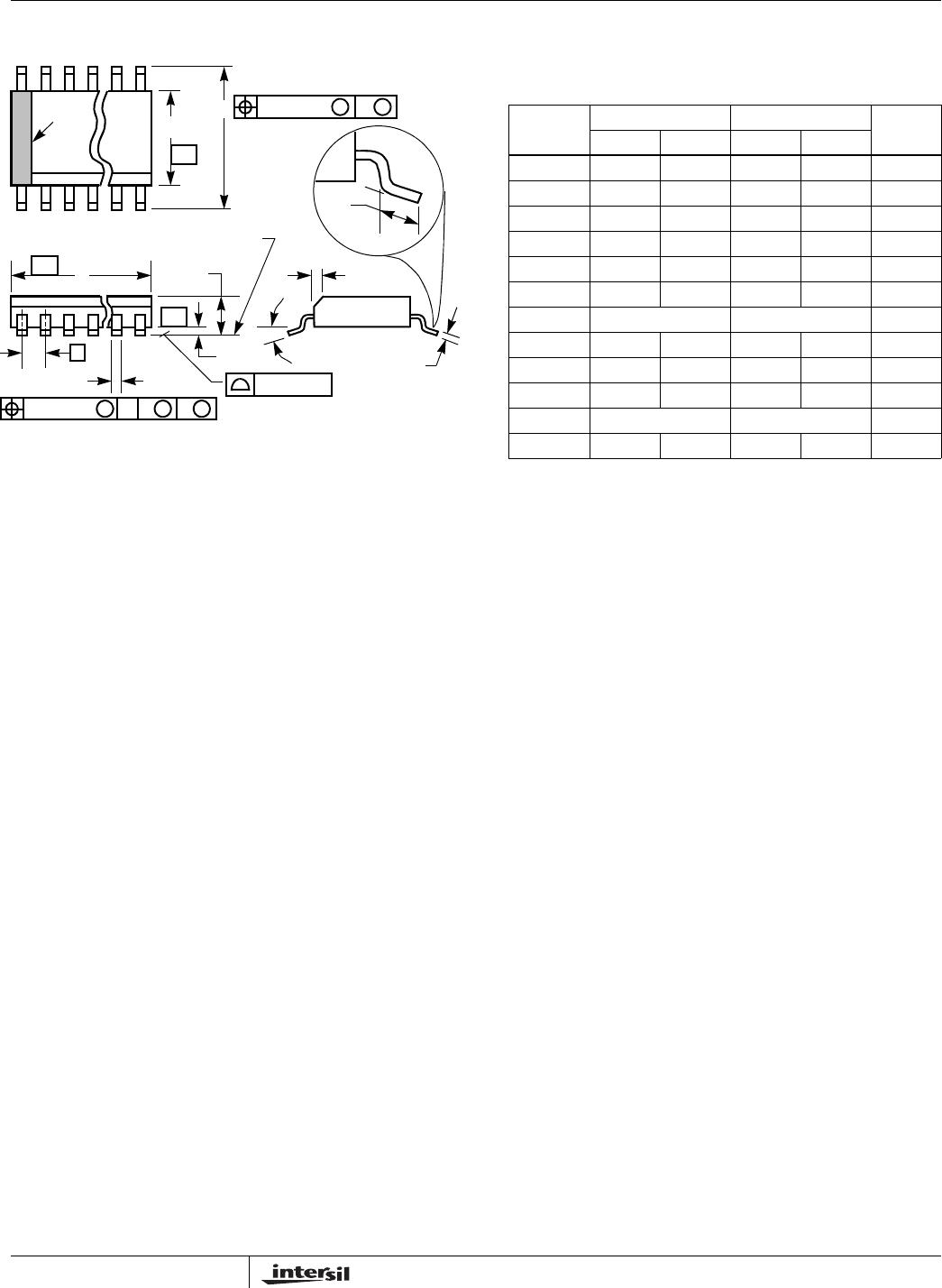
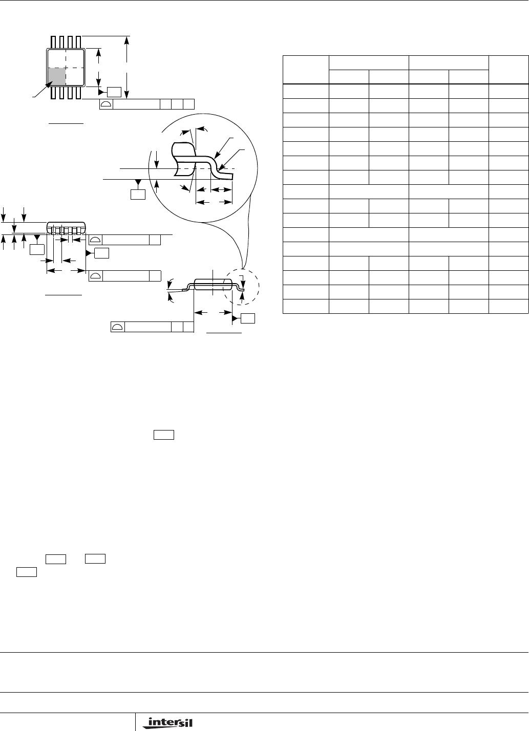
Mini Small Outline Plastic Packages (MSOP)
NOTES:
1. These package dimensions are within allowable dimensions of
JEDEC MO-187BA.
2. Dimensioning and tolerancing per ANSI Y14.5M-1994.
3. Dimension “D” does not include mold flash, protrusions or gate
burrs and are measured at Datum Plane. Mold flash, protrusion
and gate burrs shall not exceed 0.15mm (0.006 inch) per side.
4. Dimension “E1” does not include interlead flash or protrusions
and are measured at Datum Plane. Interlead flash and
protrusions shall not exceed 0.15mm (0.006 inch) per side.
5. Formed leads shall be planar with respect to one another within
0.10mm (0.004) at seating Plane.
6. “L” is the length of terminal for soldering to a substrate.
7. “N” is the number of terminal positions.
8. Terminal numbers are shown for reference only.
9. Dimension “b” does not include dambar protrusion. Allowable
dambar protrusion shall be 0.08mm (0.003 inch) total in excess
of “b” dimension at maximum material condition. Minimum space
between protrusion and adjacent lead is 0.07mm (0.0027 inch).
10. Datums and to be determined at Datum plane
.
11. Controlling dimension: MILLIMETER. Converted inch dimen-
sions are for reference only.
L
0.25
(0.010)
L1
R1
R
4X θ
4X θ
GAUGE
PLANE
SEATING
PLANE
EE1
N
12
TOP VIEW
INDEX
AREA
-C-
-B-
0.20 (0.008) A
B
C
SEATING
PLANE
0.20 (0.008) C
0.10 (0.004) C
-A-
-H-
SIDE VIEW
b
e
D
A
A1
A2
-B-
END VIEW
0.20 (0.008) C
D
E
1
C
L
C
a
- H -
-A -
- B -
- H -
M8.118 (JEDEC MO-187AA)
8 LEAD MINI SMALL OUTLINE PLASTIC PACKAGE
SYMBOL
INCHES MILLIMETERS
NOTESMIN MAX MIN MAX
A 0.037 0.043 0.94 1.10 -
A1 0.002 0.006 0.05 0.15 -
A2 0.030 0.037 0.75 0.95 -
b 0.010 0.014 0.25 0.36 9
c 0.004 0.008 0.09 0.20 -
D 0.116 0.120 2.95 3.05 3
E1 0.116 0.120 2.95 3.05 4
e 0.026 BSC 0.65 BSC -
E 0.187 0.199 4.75 5.05 -
L 0.016 0.028 0.40 0.70 6
L1 0.037 REF 0.95 REF -
N8 87
R 0.003 - 0.07 - -
R1 0.003 - 0.07 - -
0 5
o
15
o
5
o
15
o
-
α
0
o
6
o
0
o
6
o
-
Rev. 2 01/03

ISL8845AABZ

Mfr. #:
Manufacturer:
Renesas / Intersil
Description:
Switching Controllers CUR MODE PWM 50% DC 8 4V UVLO 8LD
Lifecycle:
New from this manufacturer.
Delivery:
DHL FedEx Ups TNT EMS
Payment:
T/T Paypal Visa MoneyGram Western Union