LTC6362
1
6362fa
TYPICAL APPLICATION
FEATURES DESCRIPTION
Precision, Low Power
Rail-to-Rail Input/Output
Differential Op Amp/SAR
ADC Driver
The LTC
®
6362 is a low power, low noise differential op
amp with rail-to-rail input and output swing that has been
optimized to drive low power SAR ADCs. The LTC6362
draws only 1mA of supply current in active operation, and
features a shutdown mode in which the current consump-
tion is reduced to 70μA.
The amplifier may be configured to convert a single-
ended input signal to a differential output signal, and is
capable of being operated in an inverting or noninverting
configuration.
Low offset voltage, low input bias current, and a stable
high impedance configuration make this amplifier suit-
able for use not only as an ADC driver but also earlier in
the signal chain, to convert a precision sensor signal to
a balanced (differential) signal for processing in noisy
industrial environments.
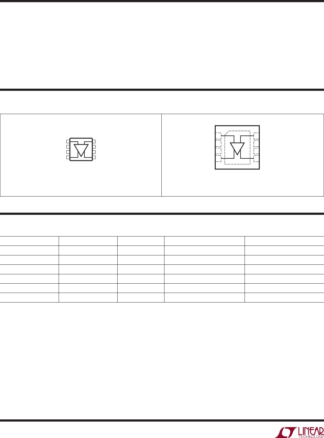
The LTC6362 is available in an 8-lead MSOP package and
also in a compact 3mm × 3mm 8-pin leadless DFN pack-
age, and operates with guaranteed specifications over a
–40°C to 125°C temperature range.
DC-Coupled Interface from a Ground-Referenced
Single-Ended Input to an LTC2379-18 SAR ADC
APPLICATIONS
n
1mA Supply Current
n
Single 2.8V to 5.25V supply
n
Fully Differential Input and Output
n
200μV Max Offset Voltage
n
260nA Max Input Bias Current
n
Fast Settling: 550ns to 18-Bit, 8V
P-P
Output
n
Low Distortion: –116dBc at 1kHz, 8V
P-P
n
Rail-to-Rail Inputs and Outputs
n
3.9nV/√Hz Input-Referred Noise
n
180MHz Gain-Bandwidth Product
n
34MHz –3dB Bandwidth
n
Low Power Shutdown: 70µA
n
8-Lead MSOP and 3mm × 3mm 8-Lead DFN Packages
n
16-Bit and 18-Bit SAR ADC Drivers
n
Single-Ended-to-Differential Conversion
n
Low Power Pipeline ADC Driver
n
Differential Line Drivers
n
Battery-Powered Instrumentation
L, LT, LTC, LTM, Linear Technology and the Linear logo are registered trademarks of Linear
Technology Corporation. All other trademarks are the property of their respective owners.
+
+
5V
3.9nF
3.9nF
3.9nF
A
IN
+
V
REF
V
DD
5V
LTC2379-18
SAR ADC
2.5V
GND
A
IN
18-BIT
1.6Msps
6362 TA01a
35.7Ω
35.7Ω
LTC6362
V
OCM
0.1µF
V
IN
1k
1k 1k
1k
SHDN
LTC6362 Driving LTC2379-18
f
IN
= 2kHz, –1dBFS, 16384-Point FFT
FREQUENCY (kHz)
0
–150
–140
AMPLITUDE (dBFS)
–120
–100
–80
0
–40
100
200
500 600 700
–20
–60
–130
–110
–90
–10
–50
–30
–70
300
400
800
6362 TA01b
V
S
= 5V, 0V
V
OUTDIFF
= 8.9V
P-P
HD2 = –116.0dBc
HD3 = –114.9dBc
SFDR = 110.1dB
THD = –108.0dB
SNR = 101.2dB
SINAD = 99.9dB
LTC6362
2
6362fa
ABSOLUTE MAXIMUM RATINGS
PIN CONFIGURATION
Total Supply Voltage (V
+
– V
) .................................5.5V
Input Current (+IN, –IN, V
OCM
, SHDN) (Note 2) ... ±10mA
Output Short-Circuit Duration (Note 3)
............ Indefinite
Operating Temperature Range (Note 4)
LTC6362C/LTC6362I ............................40°C to 85°C
LTC6362H .......................................... 40°C to 125°C
(Note 1)
1
2
3
4
–IN
V
OCM
V
+
+OUT
8
7
6
5
+IN
SHDN
V
–OUT
TOP VIEW
MS8 PACKAGE
8-LEAD PLASTIC MSOP
T
JMAX
= 150°C, θ
JA
= 273°C/W, θ
JC
= 45°C/W
TOP VIEW
9
V
DD PACKAGE
8-LEAD (3mm × 3mm) PLASTIC DFN
5
6
7
8
4
3
2
1–IN
V
OCM
V
+
+OUT
+IN
SHDN
V
–OUT
T
JMAX
= 150°C, θ
JA
= 39.7°C/W, θ
JC
= 45°C/W
EXPOSED PAD (PIN 9) IS V
, MUST BE SOLDERED TO PCB
ORDER INFORMATION
LEAD FREE FINISH TAPE AND REEL PART MARKING* PACKAGE DESCRIPTION SPECIFIED TEMPERATURE RANGE
LTC6362CMS8#PBF LTC6362CMS8#TRPBF LTGCN 8-Lead Plastic MSOP 0°C to 70°C
LTC6362IMS8#PBF LTC6362IMS8#TRPBF LTGCN 8-Lead Plastic MSOP –40°C to 85°C
LTC6362HMS8#PBF LTC6362HMS8#TRPBF LTGCN 8-Lead Plastic MSOP –40°C to 125°C
LTC6362CDD#PBF LTC6362CDD#TRPBF LGCM
8-Lead (3mm × 3mm) Plastic DFN
0°C to 70°C
LTC6362IDD#PBF LTC6362IDD#TRPBF LGCM
8-Lead (3mm × 3mm) Plastic DFN
–40°C to 85°C
LTC6362HDD#PBF LTC6362HDD#TRPBF LGCM
8-Lead (3mm × 3mm) Plastic DFN
–40°C to 125°C
Consult LTC Marketing for parts specified with wider operating temperature ranges. *The temperature grade is identified by a label on the shipping container.
Consult LTC Marketing for information on non-standard lead based finish parts.
For more information on lead free part marking, go to: http://www.linear.com/leadfree/
For more information on tape and reel specifications, go to: http://www.linear.com/tapeandreel/
Specified Temperature Range (Note 5)
LTC6362C ................................................ 0°C to 70°C
LTC6362I .............................................40°C to 85°C
LTC6362H .......................................... 40°C to 125°C
Maximum Junction Temperature
.......................... 150°C
Storage Temperature Range
.................. 65°C to 150°C
LTC6362
3
6362fa
ELECTRICAL CHARACTERISTICS
The l denotes the specifications which apply over the full operating
temperature range, otherwise specifications are at T
A
= 25°C. V
+
= 5V, V
= 0V, V
CM
= V
OCM
= V
ICM
= 2.5V, V
SHDN
= open. V
S
is defined
as (V
+
– V
). V
OUTCM
is defined as (V
+OUT
+ V
–OUT
)/2. V
ICM
is defined as (V
+IN
+ V
–IN
)/2. V
OUTDIFF
is defined as (V
+OUT
– V
–OUT
).
SYMBOL PARAMETER CONDITIONS MIN TYP MAX UNITS
V
OSDIFF
(Note 6) Differential Offset Voltage (Input Referred) V
S
= 3V
V
ICM
=1.5V
V
ICM
= 2.75V
l
l
50
65
200
350
250
600
µV
µV
µV
µV
V
S
= 5V
V
ICM
= 2.5V
V
ICM
= 4.5V
l
l
50
75
200
350
260
600
µV
µV
µV
µV
V
OSDIFF
/T (Note 7)
Differential Offset Voltage Drift (Input Referred) V
S
= 3V
V
S
= 5V
l
l
0.9
0.9
2.5
2.5
µV/°C
µV/°C
I
B
(Note 8) Input Bias Current V
S
= 3V
V
ICM
=1.5V
V
ICM
= 2.5V
l
l
±100
±75
±350
±500
±350
±850
nA
nA
nA
nA
V
S
= 5V
V
ICM
= 2.5V
V
ICM
= 4.5V
l
l
±75
±75
±260
±460
±350
±850
nA
nA
nA
nA
I
B
/T
Input Bias Current Drift V
S
= 3V
V
S
= 5V
l
l
1.1
0.9
nA/°C
nA/°C
I
OS
(Note 8) Input Offset Current V
S
= 3V
V
ICM
=1.5V
V
ICM
= 2.5V
l
l
±75
±125
±325
±650
±425
±1200
nA
nA
nA
nA
V
S
= 5V
V
ICM
=2.5V
V
ICM
= 4.5V
l
l
±75
±125
±325
±500
±425
±1200
nA
nA
nA
nA
R
IN
Input Resistance Common Mode
Differential Mode
14
32
C
IN
Input Capacitance Differential Mode 2 pF
e
n
Differential Input Noise Voltage Density f = 100kHz, Not Including R
I
/R
F
Noise 3.9 nV/√Hz
i
n
Input Noise Current Density f = 100kHz, Not Including R
I
/R
F
Noise 0.8 pA/√Hz
e
nvocm
Common Mode Noise Voltage Density f = 100kHz 14.3 nV/√Hz
V
ICMR
(Note 9) Input Common Mode Range V
S
= 3V
V
S
= 5V
l
l
0
0
3
5
V
V
CMRRI (Note 10) Input Common Mode Rejection Ratio
(Input Referred) V
ICM
/V
OSDIFF
V
S
= 3V, V
ICM
from 0V to 3V
V
S
= 5V, V
ICM
from 0V to 5V
l
l
70
73
95
98
dB
dB
CMRRIO (Note 10) Output Common Mode Rejection Ratio
(Input Referred) V
OCM
/V
OSDIFF
V
S
= 3V, V
OCM
from 0.5V to 2.5V
V
S
= 5V, V
OCM
from 0.5V to 4.5V
l
l
75
55
100
90
dB
dB
PSRR (Note 11) Differential Power Supply Rejection
(V
S
/V
OSDIFF
)
V
S
= 2.8V to 5.25V
l
80 105 dB
PSRRCM (Note 11) Output Common Mode Power Supply Rejection
(V
S
/V
OSCM
)
V
S
= 2.8V to 5.25V
l
58 72 dB

LTC6362HMS8#PBF

Mfr. #:
Manufacturer:
Analog Devices Inc.
Description:
Precision Amplifiers Low Power Differential OpAmp/ADC Driver
Lifecycle:
New from this manufacturer.
Delivery:
DHL FedEx Ups TNT EMS
Payment:
T/T Paypal Visa MoneyGram Western Union