LTC6362
14
6362fa
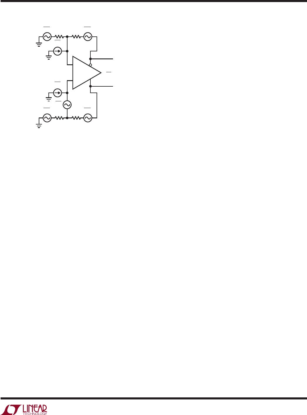
APPLICATIONS INFORMATION
To prevent degradation in stability response, it is highly
recommended that any stray capacitance at the input pins,
+IN and –IN, be kept to an absolute minimum by keeping
printed circuit connections as short as possible.
At the output, always keep in mind the differential nature of
the LTC6362, because it is critical that the load impedances
seen by both outputs (stray or intended), be as balanced
and symmetric as possible. This will help preserve the
balanced operation of the LTC6362 that minimizes the
generation of even-order harmonics and maximizes the
rejection of common mode signals and noise.
The V
OCM
pin should be bypassed to the ground plane with
a high quality 0.1µF ceramic capacitor. This will prevent
common mode signals and noise on this pin from being
inadvertently converted to differential signals and noise
by impedance mismatches both externally and internally
to the IC.
Interfacing to ADCs
When driving an ADC, an additional passive filter should be
used between the outputs of the LTC6362 and the inputs
of the ADC. Depending on the application, a single-pole
RC filter will often be sufficient. The sampling process
of ADCs creates a charge transient that is caused by the
switching in of the ADC sampling capacitor. This mo-
mentarily “shorts” the output of the amplifier as charge
is transferred between amplifier and sampling capacitor.
The amplifier must recover and settle from this load
transient before the acquisition period has ended, for a
valid representation of the input signal. The RC network
between the outputs of the driver and the inputs of the
ADC decouples the sampling transient of the ADC (see
Figure 5). The capacitance serves to provide the bulk
of the charge during the sampling process, while the
two resistors at the outputs of the LTC6362 are used to
dampen and attenuate any charge injected by the ADC.
The RC filter gives the additional benefit of band limiting
broadband output noise.
The selection of an appropriate filter depends on the specific
ADC, however the following procedure is suggested for
choosing filter component values. Begin by selecting an
appropriate RC time constant for the input signal. Gener-
ally, longer time constants improve SNR at the expense of
settling time. Output transient settling to 18-bit accuracy
will typically require over twelve RC time constants. To
select the resistor value, remember the resistors in the
decoupling network should be at least 10Ω. Keep in mind
that these resistors also serve to decouple the LTC6362
outputs from load capacitance. Too large of a resistor will
leave insufficient settling time. Too small of a resistor will
not properly dampen the load transient of the sampling
process, prolonging the time required for settling. For
lowest distortion, choose capacitors with low dielectric
absorption (such as a C0G multilayer ceramic capacitor). In
general, large capacitor values attenuate the fixed nonlinear
charge kickback, however very large capacitor values will
detrimentally load the driver at the desired input frequency
and thus cause driver distortion. Smaller input swings will
in general allow for larger filter capacitor values due to
decreased loading demands on the driver. This property
however may be limited by the particular input amplitude
dependence of differential nonlinear charge kickback for
the specific ADC used.
In some applications, placing series resistors at the inputs
of the ADC may further improve distortion performance.
These series resistors function with the ADC sampling
capacitor to filter potential ground bounce or other high
speed sampling disturbances. Additionally the resistors
limit the rise time of residual filter glitches that manage to
propagate to the driver outputs. Restricting possible glitch
propagation rise time to within the small signal bandwidth
of the driver enables less disturbed output settling.
For the specific application of LTC6362 driving the
LTC2379-18 SAR ADC in a gain of A
V
= –1 configuration,
the recommended component values of the RC filter for
varying filter bandwidths are provided in Figure 5. These
component values are chosen for optimal distortion per-
formance. Broadband output noise will vary with filter
bandwidth.