LTC6362
10
6362fa
APPLICATIONS INFORMATION
Functional Description
The LTC6362 is a low power, low noise, high DC accuracy
fully differential operational amplifier/ADC driver. The
amplifier is optimized to convert a fully differential or
single-ended signal to a low impedance, balanced differ-
ential output suitable for driving high performance, low
power differential successive approximation register (SAR)
ADCs. The balanced differential nature of the amplifier
also provides even-order harmonic distortion cancella-
tion, and low susceptibility to common mode noise (like
power supply noise).
The outputs of the LTC6362 are capable of swinging rail-
to-rail and can source or sink up to 35mA of current. The
LTC6362 is optimized for high bandwidth and low power
applications. Load capacitances above 10pF to ground or
5pF differentially should be decoupled with 10Ω to 100Ω
of series resistance from each output to prevent oscilla-
tion or ringing. Feedback should be taken directly from
the amplifier output. Higher voltage gain configurations
tend to have better capacitive drive capability than lower
gain configurations due to lower closed-loop bandwidth.
Input Pin Protection
The LTC6362 input stage is protected against differential
input voltages which exceed 1.4V by two pairs of series
diodes connected back-to-back between +IN and –IN.
Moreover, all pins have clamping diodes to both power
supplies. If any pin is driven to voltages which exceed
either supply, the current should be limited to under 10mA
to prevent damage to the IC.
SHDN Pin
The LTC6362 has a SHDN pin which when driven to within
0.8V above the negative rail, will shut down amplifier op-
eration such that only 70µA is drawn from the supplies.
Pull-down circuitry should be capable of sinking at least
4µA to guarantee complete shutdown across all condi-
tions. For normal operation, the SHDN pin should be left
floating or tied to the positive rail.
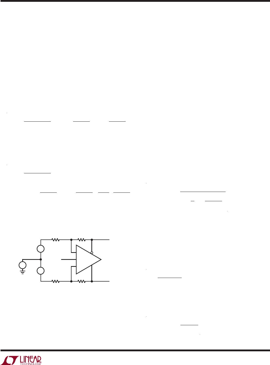
General Amplifier Applications
In Figure 1, the gain to V
OUTDIFF
from V
INP
and V
INM
is
given by:
V
OUTDIFF
= V
+OUT
V
OUT
R
F
R
I
V
INP
V
INM
( )
Note from the previous equation, the differential output
voltage (V
+OUT
– V
–OUT
) is completely independent of
input and output common mode voltages, or the voltage
at the common mode pin. This makes the LTC6362 ideally
suited for pre-amplification, level shifting and conversion
of single-ended signals to differential output signals for
driving differential input ADCs.
Output Common Mode and V
OCM
Pin
The output common mode voltage is defined as the aver-
age of the two outputs:
V
OUTCM
= V
OCM
=
V
+OUT
+ V
OUT
2
As the equation shows, the output common mode voltage
is independent of the input common mode voltage, and
is instead determined by the voltage on the V
OCM
pin, by
means of an internal common mode feedback loop.
If the V
OCM
pin is left open, an internal resistor divider
develops a default voltage of 2.5V with a 5V supply. The
V
OCM
pin can be overdriven to another voltage if desired.
For example, when driving an ADC, if the ADC makes a
reference available for setting the common mode volt-
age, it can be directly tied to the V
OCM
pin, as long as
the ADC is capable of driving the 170k input resistance
presented by the V
OCM
pin. The Electrical Characteristics
table specifies the valid range that can be applied to the
V
OCM
pin (V
OUTCMR
).
LTC6362
11
6362fa
APPLICATIONS INFORMATION
Input Common Mode Voltage Range
The LTC6362’s input common mode voltage (V
ICM
) is
defined as the average of the two input pins, V
+IN
and
V
–IN
. The inputs of the LTC6362 are capable of swinging
rail-to-rail and as such the valid range that can be used for
V
ICM
is V
to V
+
. However, due to external resistive divider
action of the gain and feedback resistors, the effective
range of signals that can be processed is even wider. The
input common mode range at the op amp inputs depends
on the circuit configuration (gain), V
OCM
and V
CM
(refer to
Figure 1). For fully differential input applications, where
V
INP
= –V
INM
, the common mode input is approximately:
V
ICM
=
V
+IN
+
V
IN
2
V
OCM
R
I
R
I
+R
F
+ V
CM
R
F
R
I
+R
F
With single-ended inputs, there is an input signal compo-
nent to the input common mode voltage. Applying only
V
INP
(setting V
INM
to zero), the input common voltage is
approximately:
V
ICM
=
V
+IN
+ V
IN
2
V
OCM
R
I
R
I
+R
F
+ V
CM
R
F
R
I
+R
F
+
V
INP
2
R
F
R
I
+R
F
This means that if, for example, the input signal (V
INP
)
is a sine, an attenuated version of that sine signal also
appears at the op amp inputs.
current follows I
B
/V
ICM
= 75nA/V, with I
B
at V
ICM
= 2.5V
typically below 75nA on a 5V supply. For common mode
voltages ranging from 1.1V below the positive supply to
0.2V below the positive supply, input bias current follows
I
B
/V
ICM
= 25nA/V, with I
B
at V
ICM
= 4.5V typically below
75nA on a 5V supply. Operating within these ranges allows
the amplifier to be used in applications with high source
resistances where errors due to voltage drops must be
minimized. For applications where V
ICM
is within 0.2V of
either rail, input bias current may reach values over 1µA.
Input Impedance and Loading Effects
The low frequency input impedance looking into the V
INP
or V
INM
input of Figure 1 depends on how the inputs are
driven. For fully differential input sources (V
INP
= –V
INM
),
the input impedance seen at either input is simply:
R
INP
= R
INM
= R
I
For single-ended inputs, because of the signal imbalance
at the input, the input impedance actually increases over
the balanced differential case. The input impedance looking
into either input is:
R
INP
=R
INM
=
R
I
1–
1
2
R
F
R
I
+R
F
Input signal sources with non-zero output impedances can
also cause feedback imbalance between the pair of feedback
networks. For the best performance, it is recommended
that the input source output impedance be compensated.
If input impedance matching is required by the source, a
termination resistor R1 should be chosen (see Figure2)
such that:
R1=
R
INM
R
S
R
INM
R
S
According to Figure 2, the input impedance looking into
the differential amp (R
INM
) reflects the single-ended source
case, given above. Also, R2 is chosen as:
R2=R1||R
S
=
R1R
S
R1+R
S
Figure 1. Definitions and Terminology
+
R
F
V
–OUT
V
+OUT
V
OCM
V
INP
V
INM
V
OCM
6362 F01
R
F
R
I
R
I
V
–IN
V
+IN
+
+
V
CM
+
Input Bias Current
Input bias current varies according to V
ICM
. For common
mode voltages ranging from 0.2V above the negative
supply to 1.1V below the positive supply, input bias
LTC6362
12
6362fa
APPLICATIONS INFORMATION
Effects of Resistor Pair Mismatch
Figure 3 shows a circuit diagram which takes into consid-
eration that real world resistors will not match perfectly.
Assuming infinite open-loop gain, the differential output
relationship is given by the equation:
V
OUT(DIFF)
= V
+OUT
– V
OUT
V
INDIFF
R
F
R
I
+ V
CM
β
β
AVG
– V
OCM
β
β
AVG
where R
F
is the average of R
F1
and R
F2
, and R
I
is the
average of R
I1
and R
I2
.
β
AVG
is defined as the average feedback factor from the
outputs to their respective inputs:
β
AVG
=
1
2
R
I1
R
I1
+R
F1
+
R
I2
R
I2
+R
F2
∆β is defined as the difference in the feedback factors:
∆β=
R
I2
R
I2
+R
F2
R
I1
R
I1
+R
F1
Here, V
CM
and V
INDIFF
are defined as the average and
the difference of the two input voltages V
INP
and V
INM
,
respectively:
V
CM
=
V
INP
+ V
INM
2
V
INDIFF
= V
INP
– V
INM
When the feedback ratios mismatch (Δβ), common mode
to differential conversion occurs. Setting the differential
input to zero (V
INDIFF
= 0), the degree of common mode
to differential conversion is given by the equation:
V
OUTDIFF
≈ (V
CM
– V
OCM
) • ∆β/β
AVG
In general, the degree of feedback pair mismatch is a
source of common mode to differential conversion of
both signals and noise. Using 0.1% resistors or better will
mitigate most problems. A low impedance ground plane
should be used as a reference for both the input signal
source and the V
OCM
pin.
Noise
The LTC6362’s differential input referred voltage and current
noise densities are 3.9nV/√Hz and 0.8pA/√Hz, respectively.
In addition to the noise generated by the amplifier, the
surrounding feedback resistors also contribute noise. A
simplified noise model is shown in Figure 4. The output
noise generated by both the amplifier and the feedback
components is given by the equation:
e
no
=
e
ni
1+
R
F
R
I
2
+2 i
n
R
F
( )
2
+ 2 e
nRI
R
F
R
I
2
+2 e
nRF
2
For example, if R
F
= R
I
= 1k, the output noise of the circuit
e
no
= 12nV/√Hz.
If the circuits surrounding the amplifier are well balanced,
common mode noise (e
nvocm
) does not appear in the dif-
ferential output noise equation given above.
Figure 2. Optimal Compensation for Signal Source Impedance
V
S
+
+
R
F
R
F
R
I
R
INM
R
S
R
I
R2 = R
S
|| R1
R1 CHOSEN SO THAT R1 || R
INM
= R
S
R2 CHOSEN TO BALANCE R1 || R
S
R1
6405 F04
+
R
F2
V
–OUT
V
+OUT
V
VOCM
V
INP
V
INM
V
OCM
6362 F03
R
F1
R
I2
R
I1
V
–IN
V
+IN
+
+
V
CM
+
Figure 3. Real-World Application with
Feedback Resistor Pair Mismatch

LTC6362IMS8#PBF

Mfr. #:
Manufacturer:
Analog Devices Inc.
Description:
Precision Amplifiers Low Power Differential OpAmp/ADC Driver
Lifecycle:
New from this manufacturer.
Delivery:
DHL FedEx Ups TNT EMS
Payment:
T/T Paypal Visa MoneyGram Western Union