LTC6362
4
6362fa
ELECTRICAL CHARACTERISTICS
The l denotes the specifications which apply over the full operating
temperature range, otherwise specifications are at T
A
= 25°C. V
+
= 5V, V
= 0V, V
CM
= V
OCM
= V
ICM
= 2.5V, V
SHDN
= open. V
S
is defined
as (V
+
– V
). V
OUTCM
is defined as (V
+OUT
+ V
–OUT
)/2. V
ICM
is defined as (V
+IN
+ V
–IN
)/2. V
OUTDIFF
is defined as (V
+OUT
– V
–OUT
).
SYMBOL PARAMETER CONDITIONS MIN TYP MAX UNITS
GCM
Common Mode Gain (V
OUTCM
/V
OCM
)
V
S
= 3V, V
OCM
from 0.5V to 2.5V
V
S
= 5V, V
OCM
from 0.5V to 4.5V
l
l
1
1
V/V
V/V
GCM
Common Mode Gain Error 100 • (GCM – 1) V
S
= 3V, V
OCM
from 0.5V to 2.5V
V
S
= 5V, V
OCM
from 0.5V to 4.5V
l
l
±0.07
±0.07
±0.16
±0.4
%
%
BAL
Output Balance (V
OUTCM
/V
OUTDIFF
) V
OUTDIFF
= 2V
Single-Ended Input
Differential Input
l
l
–57
–57
–35
–35
dB
dB
A
VOL
Open-Loop Voltage Gain 95 dB
V
OSCM
Common Mode Offset Voltage
(V
OUTCM
– V
OCM
)
V
S
= 3V
V
S
= 5V
l
l
±6
±6
±30
±30
mV
mV
V
OSCM
/T
Common Mode Offset Voltage Drift
l
45 μV/°C
V
OUTCMR
(Note 9) Output Signal Common Mode Range
(Voltage Range for the V
OCM
Pin)
V
OCM
Driven Externally, V
S
= 3V
V
OCM
Driven Externally, V
S
= 5V
l
l
0.5
0.5
2.5
4.5
V
V
V
OCM
Self-Biased Voltage at the V
OCM
Pin V
OCM
Not Connected, V
S
= 3V
V
OCM
Not Connected, V
S
= 5V
l
l
1.475
2.475
1.5
2.5
1.525
2.525
V
V
R
INVOCM
Input Resistance, V
OCM
Pin
l
110 170 230
V
OUT
Output Voltage, High, Either Output Pin I
L
= 0mA, V
S
= 3V
I
L
= –5mA, V
S
= 3V
l
l
2.85
2.75
2.93
2.85
V
V
I
L
= 0mA, V
S
= 5V
I
L
= –5mA, V
S
= 5V
l
l
4.8
4.7
4.93
4.85
V
V
Output Voltage, Low , Either Output Pin I
L
= 0mA, V
S
= 3V
I
L
= 5mA, V
S
= 3V
l
l
0.05
0.13
0.15
0.3
V
V
I
L
= 0mA, V
S
= 5V
I
L
= 5mA, V
S
= 5V
l
l
0.05
0.13
0.2
0.4
V
V
I
SC
Output Short-Circuit Current, Either Output Pin V
S
= 3V
V
S
= 5V
l
l
13
15
25
35
mA
mA
SR Slew Rate Differential 8V
P-P
Output 45 V/μs
GBWP Gain-Bandwidth Product f
TEST
= 200kHz
l
145
90
180 MHz
MHz
f
–3dB
–3dB Bandwidth R
I
= R
F
= 1k 34 MHz
HD2/HD3 2nd/3rd Order Harmonic Distortion
Single-Ended Input
f = 1kHz, V
OUT
= 8V
P-P
f = 10kHz, V
OUT
= 8V
P-P
f = 100kHz, V
OUT
= 8V
P-P
–120/–116
–106/–103
–84/–76
dBc
dBc
dBc
t
s
Settling Time to a 2V
P-P
Output Step 0.1%
0.01%
0.0015% (16-Bit)
4ppm (18-Bit)
160
180
230
440
ns
ns
ns
ns
Settling Time to a 8V
P-P
Output Step 0.1%
0.01%
0.0015% (16-Bit)
4ppm (18-Bit)
230
300
460
550
ns
ns
ns
ns
V
S
(Note 12) Supply Voltage Range
l
2.8 5.25 V
I
S
Supply Current V
S
= 3V, Active
l
0.9 0.96
1.05
mA
mA
V
S
= 3V, Shutdown
l
55 130 µA
V
S
= 5V, Active
l
1 1.06
1.18
mA
mA
V
S
= 5V, Shutdown
l
70 140 µA
LTC6362
5
6362fa
ELECTRICAL CHARACTERISTICS
The l denotes the specifications which apply over the full operating
temperature range, otherwise specifications are at T
A
= 25°C. V
+
= 5V, V
= 0V, V
CM
= V
OCM
= V
ICM
= 2.5V, V
SHDN
= open. V
S
is defined
as (V
+
– V
). V
OUTCM
is defined as (V
+OUT
+ V
–OUT
)/2. V
ICM
is defined as (V
+IN
+ V
–IN
)/2. V
OUTDIFF
is defined as (V
+OUT
– V
–OUT
).
Note 1: Stresses beyond those listed under Absolute Maximum Ratings
may cause permanent damage to the device. Exposure to any Absolute
Maximum Rating condition for extended periods may affect device
reliability and lifetime.
Note 2: Input pins (+IN, –IN, V
OCM
and SHDN) are protected by steering
diodes to either supply. If the inputs should exceed either supply voltage,
the input current should be limited to less than 10mA. In addition, the
inputs +IN, –IN are protected by a pair of back-to-back diodes. If the
differential input voltage exceeds 1.4V, the input current should be limited
to less than 10mA.
Note 3: A heat sink may be required to keep the junction temperature
below the absolute maximum rating when the output is shorted
indefinitely.
Note 4: The LTC6362C and LTC6362I are guaranteed functional over
the operating temperature range of –40°C to 85°C. The LTC6362H is
guaranteed functional over the operating temperature range of –40°C to
125°C.
Note 5: The LTC6362C is guaranteed to meet specified performance from
0°C to 70°C.The LTC6362I is guaranteed to meet specified performance
from –40°C to 85°C. The LTC6362C is designed, characterized and
expected to meet specified performance from –40°C to 85°C, but is not
tested or QA sampled at these temperatures. The LTC6362H is guaranteed
to meet specified performance from –40°C to 125°C.
Note 6: Differential input referred offset voltage includes offset due to
input offset current across 1k source resistance.
Note 7: Maximum differential input referred offset voltage drift is
determined by a large sampling of typical parts. Drift is not guaranteed by
test or QA sampled at this value.
Note 8: Input bias current is defined as the maximum of the input currents
flowing into either of the input pins (–IN and +IN). Input Offset current is
defined as the difference between the input currents (I
OS
= I
B
+
– I
B
).
Note 9: Input common mode range is tested by verifying that at the limits
stated in the Electrical Characteristics table, the differential offset (V
OSDIFF
)
and common mode offset (V
OSCM
) have not deviated by more than ±1mV
and ±35mV respectively compared to the V
ICM
= 2.5V (at V
S
= 5V) and
V
ICM
= 1.5V (at V
S
= 3V) cases.
Output common mode range is tested by verifying that at the limits stated
in the Electrical Characteristics table, the common mode offset (V
OSCM
)
has not deviated by more than ±15mV compared to the V
OCM
= 2.5V
(at V
S
= 5V) and V
OCM
= 1.5V (at V
S
= 3V) cases.
Note 10: Input CMRR is defined as the ratio of the change in the input
common mode voltage at the pins +IN or –IN to the change in differential
input referred offset voltage. Output CMRR is defined as the ratio of
the change in the voltage at the V
OCM
pin to the change in differential
input referred offset voltage. This specification is strongly dependent on
feedback ratio matching between the two outputs and their respective
inputs and it is difficult to measure actual amplifier performance (see
Effects of Resistor Pair Mismatch in the Applications Information section
of this data sheet). For a better indicator of actual amplifier performance
independent of feedback component matching, refer to the PSRR
specification.
Note 11: Differential power supply rejection (PSRR) is defined as the
ratio of the change in supply voltage to the change in differential input
referred offset voltage. Common mode power supply rejection (PSRRCM)
is defined as the ratio of the change in supply voltage to the change in the
common mode offset voltage.
Note 12: Supply voltage range is guaranteed by power supply rejection
ratio test.
SYMBOL PARAMETER CONDITIONS MIN TYP MAX UNITS
V
IL
SHDN Input Logic Low
l
0.8 V
V
IH
SHDN Input Logic High
l
2 V
t
ON
Turn-On Time 2 μs
t
OFF
Turn-Off Time 2 μs
LTC6362
6
6362fa
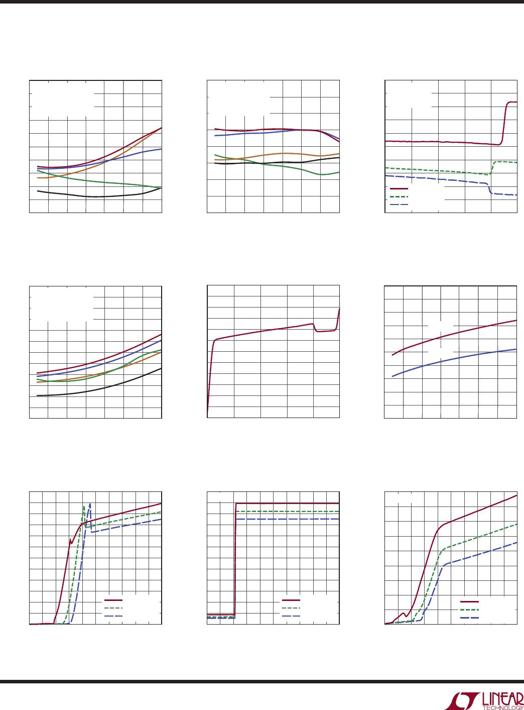
TYPICAL PERFORMANCE CHARACTERISTICS
Supply Current vs SHDN Voltage
Shutdown Supply Current
vs Supply Voltage
Input Bias Current vs Input
Common Mode Voltage Supply Current vs Temperature
Supply Current
vs Supply Voltage
Common Mode Offset Voltage
vs Temperature
TEMPERATURE (°C)
–50
COMMON MODE OFFSET VOLTAGE (mV)
–5
10
15
0
50
75
6362 G04
–10
5
0
–15
–25
25
100
125
V
S
= ±2.5V
V
ICM
= 0V
V
OCM
= 0V
FIVE TYPICAL UNITS
INPUT COMMON MODE VOLTAGE (V)
0
INPUT BIAS CURRENT (nA)
–400
0
400
800
V
S
= 5V
4
6362 G05
–800
–1200
–600
–200
200
600
–1000
–1400
–1600
1
2
3
5
TEMPERATURE (°C)
50
0.7
SUPPLY CURRENT (mA)
0.9
1.2
0
50
75
6362 G06
0.8
1.1
1.0
25
25
100
125
V
S
= 5V
V
S
= 3V
SUPPLY VOLTAGE (V)
0
SUPPLY CURRENT (mA)
0.6
0.8
1.0
1.2
4
6362 G07
0.4
0.2
0
1
2
3
5
T
A
= 125°C
T
A
= 25°C
T
A
= –40°C
SHDN VOLTAGE (V)
0
SUPPLY CURRENT (mA)
0.6
0.8
1.0
1.2
4
6362 G08
0.4
0.2
0
1
2
3
5
T
A
= 125°C
T
A
= 25°C
T
A
= –40°C
V
S
= 5V
SUPPLY VOLTAGE (V)
0
0
10
30
40
50
3 4
6362 G09
20
1 2 5
60
70
80
T
A
= 125°C
T
A
= 25°C
T
A
= –40°C
V
SHDN
= V
Differential Input Offset Voltage
vs Temperature
Differential Input Offset Voltage
vs Input Common Mode Voltage
Input Offset Current
vs Temperature
TEMPERATURE (°C)
50
–200
DIFFERENTIAL INPUT OFFSET VOLTAGE (µV)
–150
–50
0
50
300
150
0
50
75
6362 G01
–100
200
250
100
25
25
100
125
V
S
= ±2.5V
V
ICM
= 0V
V
OCM
= 0V
FIVE TYPICAL UNITS
TEMPERATURE (°C)
–50
INPUT OFFSET CURRENT (nA)
75
25
6362 G02
0
–50
–25 0 50
–75
–100
100
50
25
–25
75 100 125
V
S
= ±2.5V
V
ICM
= 0V
V
OCM
= 0V
FIVE TYPICAL UNITS
INPUT COMMON MODE VOLTAGE (V)
0
DIFFERENTIAL INPUT OFFSET VOLTAGE (µV)
100
200
300
4
6362 G03
0
–100
50
150
250
–50
–150
–200
1
2
3
5
T
A
= 125°C
T
A
= 25°C
T
A
= –40°C
V
S
= 5V, 0V
V
OCM
= 2.5V
TYPICAL UNIT

LTC6362IMS8#PBF

Mfr. #:
Manufacturer:
Analog Devices Inc.
Description:
Precision Amplifiers Low Power Differential OpAmp/ADC Driver
Lifecycle:
New from this manufacturer.
Delivery:
DHL FedEx Ups TNT EMS
Payment:
T/T Paypal Visa MoneyGram Western Union