ICS552-02
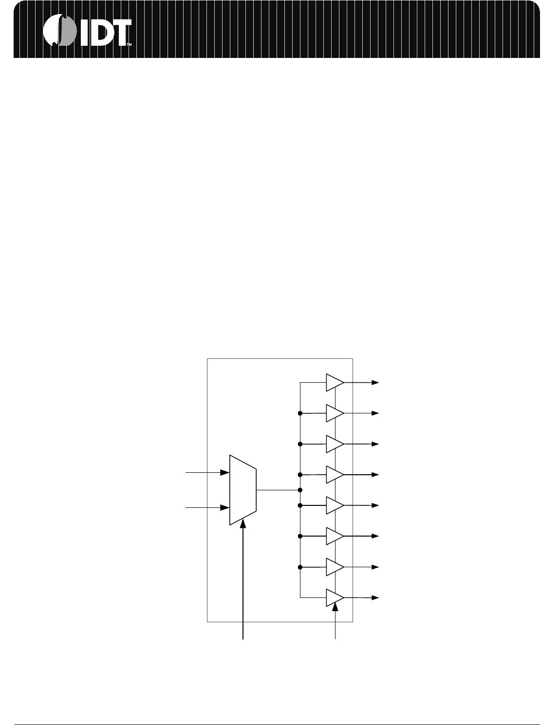
LOW SKEW 2 INPUT MUX AND 1 TO 8 CLOCK BUFFER CLOCK MUX AND BUFFER
IDT™ / ICS™
LOW SKEW 2 INPUT MUX AND 1 TO 8 CLOCK BUFFER 3
ICS552-02 REV K 092309
Absolute Maximum Ratings
Stresses above the ratings listed below can cause permanent damage to the ICS552-02. These ratings,
which are standard values for IDT commercially rated parts, are stress ratings only. Functional operation of
the device at these or any other conditions above those indicated in the operational sections of the
specifications is not implied. Exposure to absolute maximum rating conditions for extended periods can
affect product reliability. Electrical parameters are guaranteed only over the recommended operating
temperature range.
Recommended Operation Conditions
DC Electrical Characteristics
VDD=2.5 V ±5%
, Ambient temperature -40 to +85 ° C, unless stated otherwise
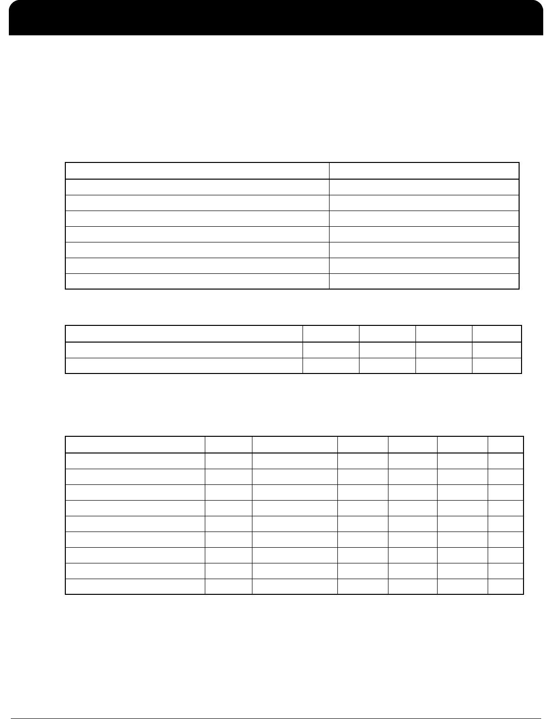
Item Rating
Supply Voltage, VDD 7 V
SELA, OE, and all Outputs -0.5 V to VDD+0.5 V
INA and INB -0.5V to 5.5V
Ambient Operating Temperature -40 to +85 ° C
Storage Temperature -65 to +150 ° C
Junction Temperature 175 ° C
Soldering Temperature 260 ° C
Parameter Min. Typ. Max. Units
Ambient Operating Temperature -40 – +85 ° C
Power Supply Voltage (measured in respect to GND) +2.375 +5.25 V
Parameter Symbol Conditions Min. Typ. Max. Units
Operating Voltage VDD 2.375 2.625 V
Input High Voltage, INA, INB V
IH
Note 1 VDD/2+0.5 5.5 V
Input Low Voltage, INA, INB V
IL
Note 1 VDD/2-0.5 V
Input High Voltage, OE, SELA V
IH
1.8 VDD V
Input Low Voltage, OE, SELA V
IL
0.7 V
Output High Voltage V
OH
I
OH
= -16 mA 2 V
Output Low Voltage V
OL
I
OL
= 16 mA 0.4 V
Operating Supply Current IDD No load, 135 MHz 35 mA
Short Circuit Current I
OS
Each output 60 mA