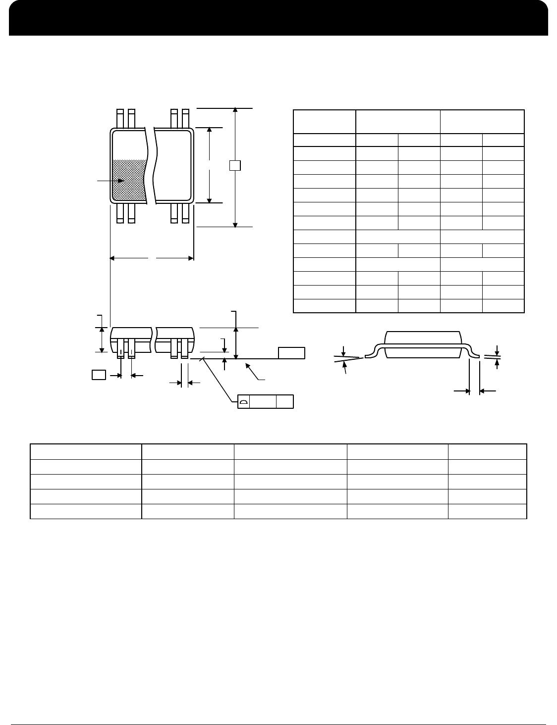
552G-02ILNT

ICS552-02
LOW SKEW 2 INPUT MUX AND 1 TO 8 CLOCK BUFFER CLOCK MUX AND BUFFER
IDT / ICS™
LOW SKEW 2 INPUT MUX AND 1 TO 8 CLOCK BUFFER 4
ICS552-02 REV K 092309
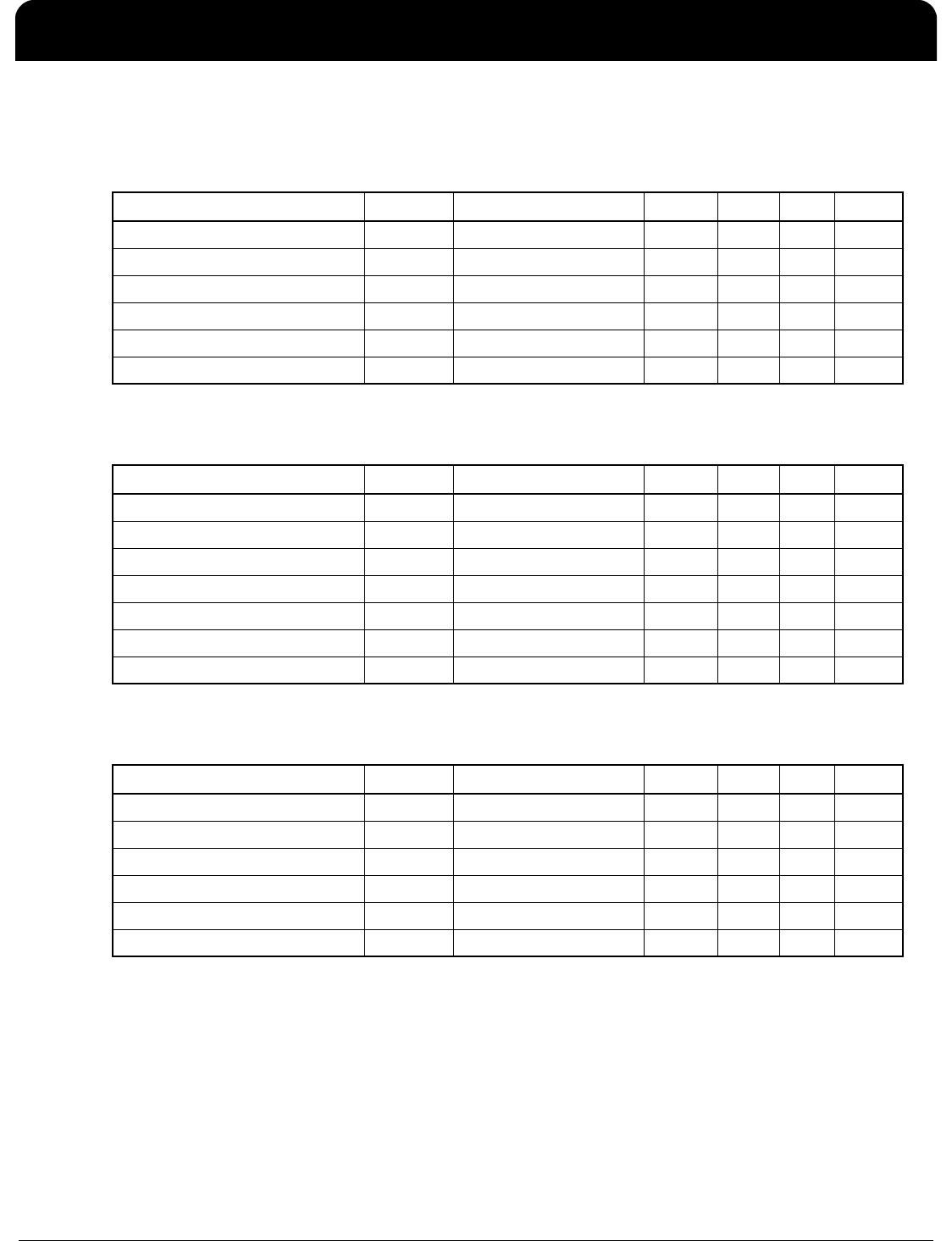
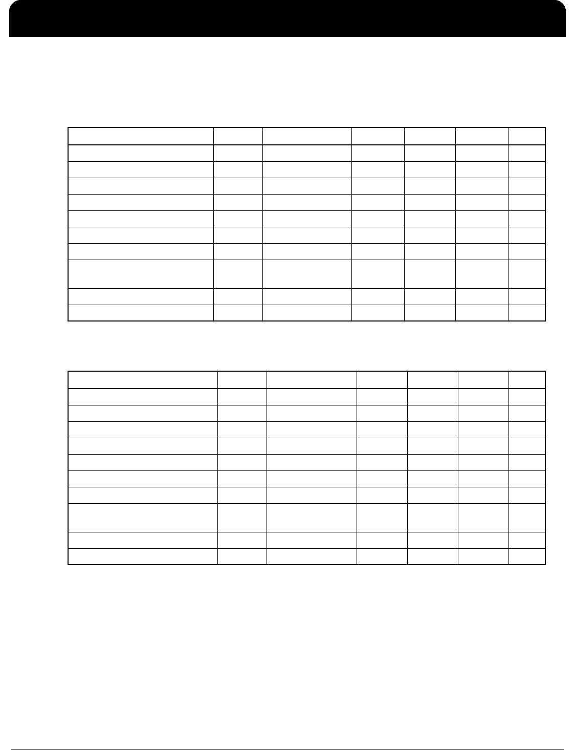
DC Electrical Characteristics (continued)
VDD=3.3 V ±5%
, Ambient temperature -40 to +85 ° C, unless stated otherwise
VDD=5 V ±5%
, Ambient temperature -40 to +85 ° C, unless stated otherwise
Note: 1. Nominal switching threshold is VDD/2
Parameter Symbol Conditions Min. Typ. Max. Units
Operating Voltage VDD 3.135 3.465 V
Input High Voltage, INA, INB V
IH
Note 1 VDD/2+0.7 5.5 V
Input Low Voltage, INA, INB V
IL
Note 1 VDD/2-0.7 V
Input High Voltage, OE, SELA V
IH
2 VDD V
Input Low Voltage, OE, SELA V
IL
0.8 V
Output High Voltage V
OH
I
OH
= -25 mA 2.4 V
Output Low Voltage V
OL
I
OH
= 25 mA 0.4 V
Output High Voltage (CMOS
Level)
V
OH
I
OH
= -12 mA VDD-0.4 V
Operating Supply Current IDD No load, 135 MHz 50 mA
Short Circuit Current I
OS
Each output 80 mA
Parameter Symbol Conditions Min. Typ. Max. Units
Operating Voltage VDD 4.75 5.25 V
Input High Voltage, INA, INB V
IH
Note 1 VDD/2+1 5.5 V
Input Low Voltage, INA, INB V
IL
Note 1 VDD/2-1 V
Input High Voltage, OE, SELA V
IH
2 VDD V
Input Low Voltage, OE, SELA V
IL
0.8 V
Output High Voltage V
OH
I
OH
= -35 mA 2.4 V
Output Low Voltage V
OL
I
OL
= 35 mA 0.4 V
Output High Voltage (CMOS
Level)
V
OH
I
OH
= -12 mA VDD-0.4 V
Operating Supply Current IDD No load, 135 MHz 85 mA
Short Circuit Current I
OS
Each output 100 mA
ICS552-02
LOW SKEW 2 INPUT MUX AND 1 TO 8 CLOCK BUFFER CLOCK MUX AND BUFFER
IDT / ICS™
LOW SKEW 2 INPUT MUX AND 1 TO 8 CLOCK BUFFER 5
ICS552-02 REV K 092309
AC Electrical Characteristics
VDD = 2.5V ±5%
, Ambient Temperature -40 to +85 ° C, unless stated otherwise
VDD = 3.3V ±5%
, Ambient Temperature -40 to +85 ° C, unless stated otherwise
VDD = 5.0V ±5%
, Ambient Temperature -40 to +85 ° C, unless stated otherwise
Notes: 1. With rail-to-rail input clock.
2. Between any two outputs with equal loading.
3. Propagation delay matching through the part.
4. Duty cycle on outputs will match incoming clock duty cycle. Consult IDT for tight duty cycle clock
generators.
Parameter Symbol Conditions Min. Typ. Max. Units
Input Frequency 0 200 MHz
Output Rise Time t
OR
0.8 to 2.0 V, C
L
=15 pF 1.0 1.5 ns
Output Fall Time t
OF
2.0 to 0.8 V, C
L
=15 pF 1.0 1.5 ns
Propagation Delay Note 1 3.5 ns
Output to output skew Note 2 Rising edges at VDD/2 0 50 ps
Input A to Input B skew Note 3 0 50 ps
Parameter Symbol Conditions Min. Typ. Max. Units
Input Frequency 0 200 MHz
Output Rise Time t
OR
0.8 to 2.0 V, C
L
=15 pF 0.6 1.0 ns
Output Fall Time t
OF
2.0 to 0.8 V, C
L
=15 pF 0.6 1.0 ns
Propagation Delay Note 1 2.0 3.0 5.5 ns
Output to output skew Note 2 Rising edges at VDD/2 0 50 ps
Input A to Input B skew Note 3 0 50 ps
Part to Part Skew 3.5 ns
Parameter Symbol Conditions Min. Typ. Max. Units
Input Frequency 0 200 MHz
Output Rise Time t
OR
0.8 to 2.0 V, C
L
=15 pF 0.3 0.7 ns
Output Fall Time t
OF
2.0 to 0.8 V, C
L
=15 pF 0.3 0.7 ns
Propagation Delay Note 1 2.8 ns
Output to output skew Note 2 Rising edges at VDD/2 0 50 ps
Input A to Input B skew Note 3 0 50 ps
ICS552-02
LOW SKEW 2 INPUT MUX AND 1 TO 8 CLOCK BUFFER CLOCK MUX AND BUFFER
IDT / ICS™
LOW SKEW 2 INPUT MUX AND 1 TO 8 CLOCK BUFFER 6
ICS552-02 REV K 092309
Package Outline and Package Dimensions
(16 pin TSSOP, 4.40 mm Body, 0.65 mm Pitch)
Package dimensions are kept current with JEDEC Publication No. 95, MO-153
Ordering Information
*NOTE: EOL for non-green parts to occur on 5/13/10 per PDN U-09-01
Parts that are ordered with an “LN” suffix to the part number are the Pb-Free configuration and are RoHS
compliant.
While the information presented herein has been checked for both accuracy and reliability, Integrated Device Technology (IDT)
assumes no responsibility for either its use or for the infringement of any patents or other rights of third parties, which would result
from its use. No other circuits, patents, or licenses are implied. This product is intended for use in normal commercial
applications. Any other applications such as those requiring extended temperature range, high reliability, or other extraordinary
environmental requirements are not recommended without additional processing by IDT. IDT reserves the right to change any
circuitry or specifications without notice. IDT does not authorize or warrant any IDT product for use in life support devices or
critical medical instruments.
Part / Order Number Marking Shipping Packaging Package Temperature
552G-02I* 552G-02I Tubes 16-pin TSSOP -40 to +85 ° C
552G-02IT* 552G-02I Tape and Reel 16-pin TSSOP -40 to +85 ° C
552G-02ILN 552G02IN Tubes 16-pin TSSOP -40 to +85 ° C
552G-02ILNT 552G02IN Tape and Reel 16-pin TSSOP -40 to +85 ° C
IND EX
AREA
1 2
16
D
E1
E
SE A T ING
PLANE
A
1
A
A
2
e
- C -
b
aaa
C
α
c
L
Millimeters Inches
Symbol Min Max Min Max
A -- 1.20 -- 0.047
A1 0.05 0.15 0.002 0.006
A2 0.80 1.05 0.032 0.041
b 0.19 0.30 0.007 0.012
C 0.09 0.20 0.0035 0.008
D 4.90 5.1 0.193 0.201
E 6.40 BASIC 0.252 BASIC
E1 4.30 4.50 0.169 0.177
e 0.65 Basic 0.0256 Basic
L 0.45 0.75 0.018 0.030
α
0
°
8
°
0
°
8
°
aaa -- 0.10 -- 0.004

552G-02ILNT

Mfr. #:
Manufacturer:
IDT
Description:
Clock Buffer OSCILLATOR, BUFFER AND MULTIPLIER
Lifecycle:
New from this manufacturer.
Delivery:
DHL FedEx Ups TNT EMS
Payment:
T/T Paypal Visa MoneyGram Western Union

Products related to this Datasheet