ADCMP356YKSZ-REEL7

ADCMP350/ADCMP354/ADCMP356 Data Sheet
Rev. D | Page 4 of 12
ABSOLUTE MAXIMUM RATINGS
T
A
= 25°C, unless otherwise noted.
Table 3.
Parameter Rating
V
CC
−0.3 V to +6 V
V
IN
−0.3 V to +25 V
OUT (Open-Drain) −0.3 V to +25 V
OUT (Push-Pull) −0.3 V to (V
CC
+ 0.3 V)
Operating Temperature Range −40°C to +125°C
Storage Temperature Range 65°C to +150°C
θ
JA
Thermal Impedance, SC70
146°C/W
Lead Temperature
Soldering (10 sec) 300°C
Vapor Phase (60 sec) 215°C
Infrared (15 sec) 220°C
Stresses at or above those listed under Absolute Maximum
Ratings may cause permanent damage to the product. This is a
stress rating only; functional operation of the product at these
or any other conditions above those indicated in the operational
section of this specification is not implied. Operation beyond
the maximum operating conditions for extended periods may
affect product reliability.
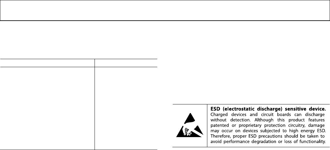
ESD CAUTION
Data Sheet ADCMP350/ADCMP354/ADCMP356
Rev. D | Page 5 of 12
PIN CONFIGURATION AND FUNCTION DESCRIPTIONS
4
ADCMP350/
ADCMP354/
ADCMP356
GND
OU
T
V
CC
V
IN
1
32
05112-002
Figure 3. Pin Configuration
Table 4. Pin Function Descriptions
Pin No. Mnemonic Description
1 V
IN
Monitors Analog Input Voltage. Connected to inverting or noninverting input depending on the model number.
2 GND Ground.
3 OUT Digital Output. Open-drain or push-pull options depending on the model number.
4 V
CC
Power Supply.
ADCMP350/ADCMP354/ADCMP356 Data Sheet
Rev. D | Page 6 of 12
TYPICAL PERFORMANCE CHARACTERISTICS
7.0
7.5
8.0
8.5
9.0
9.5
10.0
10.5
11.0
2.25 2.55 2.85 3.15 3.45 5.55
V
CC
(V)
I
CC
(µA)
05112-003
3.75 4.05 4.35 4.65
4.95 5.25
T
A
+125°C
T
A
+25°C
T
A
–40°C
T
A
+85°C
Figure 4. I
CC
vs. V
CC
over Temperature
500
540
560
580
600
620
640
660
680
700
40
–25
–10
5 20 35
50 65 80 95 110
125
TEMPERATURE (
°C)
V
TRIP
(mV)
05112-004
V
TRIP
TRIP RISING
520
V
TRIP
TRIP FALLING
Figure 5. V
IN
Trip Threshold vs. Temperature (V
CC
= 3.3 V)
0
4
6
8
10
12
14
16
18
20
–40
25 –10 5 20 35 50
65 80 95 110 125
TEMPERATURE (°C)
HYSTERESIS (mV)
05112-005
2
HYSTERESIS
Figure 6. V
IN
Trip Hysteresis vs. Temperature
0
4
6
8
10
12
14
16
18
20
0 2
4 6
8
22
V
IN
(V)
SUPPLY CURRENT (
µA)
05112-006
2
10
12 14 16 18 20
Figure 7. Supply Current vs. Input Voltage (V
IN
)
0
40
60
80
100
120
140
160
180
200
0
2 4
6 8 22
V
IN
(V)
IN LEAKAGE (µA)
05112-007
20
10 12 14 16
18
20
T
A
= +125°C
T
A
= +85°C
T
A
= +25
°C
T
A
= –
40
°C
Figure 8. Input Leakage vs. Input Voltage (V
IN
)
05112-019
0
0.1
0.2
0.3
0.4
0.5
0.6
0.7
0.8
0.9
1.0
0 0.3 0.6 0.9 1.2 1.5 1.8 2.1 2.4 2.7 3.0 3.3
V
IN
(V)
T
A
= 25°C
Figure 9. V
IN
Leakage Current vs. V
IN
Voltage (V
CC
= 3.8 V)

ADCMP356YKSZ-REEL7

Mfr. #:
Manufacturer:
Analog Devices Inc.
Description:
Analog Comparators 0.6V Ref w/ PushPull Active-Hi Out
Lifecycle:
New from this manufacturer.
Delivery:
DHL FedEx Ups TNT EMS
Payment:
T/T Paypal Visa MoneyGram Western Union