ADCMP356YKSZ-REEL7

Data Sheet ADCMP350/ADCMP354/ADCMP356
Rev. D | Page 7 of 12
110
120
140
150
160
170
180
190
200
IN LEAKAGE (µA)
05112-008
130
2.25
2.55 2.85 3.15 3.45 5.55
V
CC
(V)
3.75 4.05 4.35 4.65 4.95 5.25
T
A
= +125
°C
T
A
= +85°
C
T
A
= –40°C
T
A
= +25°C
100
Figure 10. Input Leakage vs. Supply Voltage, V
CC
(V
IN
= 22 V)
520
540
580
600
620
640
660
680
700
V
TRIP
(mV)
05112-009
560
2.25 2.55 2.85 3.15 3.45 5.55
V
CC
(V)
3.75 4.05 4.35 4.65 4.95 5.25
500
V
TRIP
RISING
V
TRIP
FALLING
Figure 11. V
IN
Trip Threshold vs. V
CC
2
4
8
10
12
14
16
18
20
HYSTERESIS (mV)
05112-020
6
2.25 2.55 2.85 3.15 3.45 5.55
V
CC
(V)
3.75 4.05 4.35 4.65
4.95 5.25
0
HYSTERESIS
Figure 12. V
IN
Trip Hysteresis vs. V
CC
0.1
1
10
100
1000
10000
0.01
0.1
10
OUTPUT SINK CURRENT (mA)
OUTPUT VOLTAGE (mV)
05112-010
1
T
A
= +125°C
T
A
= +85°C
T
A
= +25°
C
T
A
=
–40°C
Figure 13. Output Voltage vs. Output Sink Current
20
40
80
100
120
OUTPUT LOW VOLTAGE (mV)
05112-011
60
2.25 2.40 2.70 3.00 3.30
5.50
SUPPLY VOLTAGE (V)
3.60 3.90 4.20 4.50
4.80 5.20
0
Figure 14. Output Low Voltage vs. Supply Voltage (I
SINK
= 500 μA)
20
40
80
100
120
140
160
180
200
FALL TIME (ns)
05112-012
60
2.25 2.40 2.70 3.00 3.30 5.50
SUPPLY VOLTAGE (V)
3.60 3.90 4.20 4.50 4.80 5.20
0
RISE TIME
FALL TIME
Figure 15. Fall Time vs. Supply Voltage
ADCMP350/ADCMP354/ADCMP356 Data Sheet
Rev. D | Page 8 of 12
10
20
40
50
60
70
80
90
100
SHORT-CIRCUIT SINK CURRENT (mA)
05112-013
30
2.25 2.40 2.70 3.00 3.30
5.50
SUPPLY VOLTAGE (V)
3.60
3.90 4.20
4.50 4.80
5.20
0
Figure 16. Short-Circuit Sink Current vs. Supply Voltage
(V
CC
= 3.3 V, Push-Pull Only)
5
15
20
25
10 80 90 100 110 130
INPUT OVERDRIVE (mV)
PROPAGATION DELAY (µs)
05112-014
0
10
12070
605040
3020
t
PLH
t
PHL
Figure 17. Propagation Delay vs. Input Overdrive (V
CC
= 3.3 V, Push-Pull Only)
05112-015
CH1 20mV/DIV
CH2 1.00V/DIV
TIMEBASE: 10
µs/DIV
1
2
CH1 = VIN
CH2 = VOUT
Figure 18. Propagation Delay Timing, 10 mV Overdrive
05112-016
CH1 100mV/DIV
CH2 1.00V/DIV
TIMEBASE: 10
µ
s/DIV
1
2
CH1 = VIN
CH2 = VOUT
Figure 19. Propagation Delay Timing, 100 mV Overdrive
Data Sheet ADCMP350/ADCMP354/ADCMP356
Rev. D | Page 9 of 12
APPLICATIONS INFORMATION
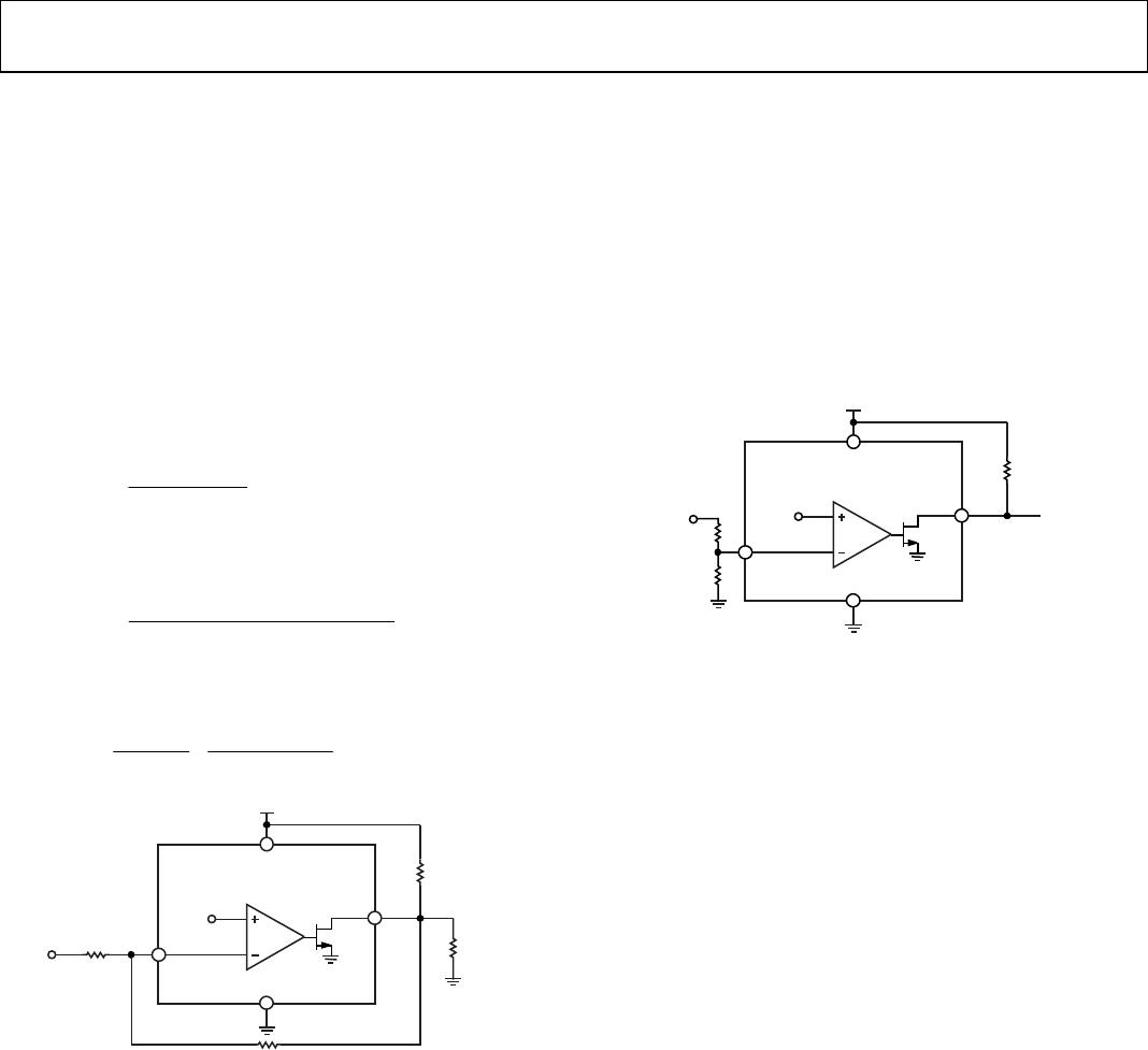
ADDING HYSTERESIS
To prevent oscillations at the output caused by noise or slowly
moving signals passing the switching threshold, positive feedback
can be used to add hysteresis to the noninverting parts
(ADCMP354 and ADCMP356).
For the noninverting configuration shown in Figure 20, two
resistors are used to create different switching thresholds,
depending on whether the input signal is increasing or decreasing
in magnitude. When the input voltage is increasing, the threshold is
above V
REF
, and when it is decreasing, the threshold is below V
REF
.
The upper input threshold level is given by

R2
R2R1V
REF
IN_HI
V
where V
REF
= 0.6 V, assuming R
LOAD
>> R2, R
PULLUP
The lower input threshold level is given by
PULLUP
CC
PULLUPREF
RR2
R1VRR2R1V
IN_LO
V
The hysteresis is the difference between these voltage levels and
is given by
PULLUP
CCREF
REF
HYS
RR2
VVR1
R2
R1V
V
ADCMP354
OUT
V
CC
= 5V
R
PULLUP
R
LOAD
R2
R1
V
IN
V
REF
= 0.6V
05112-022
Figure 20. Noninverting Comparator Configuration with Added Hysteresis
VOLTAGE DETECTOR
The ADCMP350/ADCMP354/ADCMP356 can be used to
monitor voltages, such as battery monitoring or threshold
detectors. Using a resistor divider at the input to select the
appropriate trip voltage, the comparator can be configured
to give a logic output when the input passes that threshold.
Figure 21 shows the typical configuration of the ADCMP354
for monitoring a supply to indicate that the voltage is above a
certain level.
ADCMP354
OUT
V
CC
= 5V
R
PULLUP
R1
R2
V
IN
V
REF
= 0.6V
05112-023
Figure 21. Voltage Detector Application

ADCMP356YKSZ-REEL7

Mfr. #:
Manufacturer:
Analog Devices Inc.
Description:
Analog Comparators 0.6V Ref w/ PushPull Active-Hi Out
Lifecycle:
New from this manufacturer.
Delivery:
DHL FedEx Ups TNT EMS
Payment:
T/T Paypal Visa MoneyGram Western Union