1 of 21 011006
FEATURES
§ Processor-controlled or standalone solid-
state oscillator
§ Frequency changes on-the-fly
§ Dual low-jitter, synchronous fixed
frequency outputs
§ 2-wire serial interface
§ Frequency outputs 8.1kHz to 133MHz
§ ±0.5% variation over temp (+25°C to
+70°C)
§ ±0.5% initial tolerance
§ Nonvolatile (NV) frequency settings
§ Single 5V supply
§ No external components
§ Power-down mode
§ Synchronous output gating
STANDARD FREQUENCY OPTION
Note: x denotes package option
DS1077x-133 133.333MHz to 16.2kHz
DS1077x-125 125.000MHz to 15.2kHz
DS1077x-120 120.000MHz to 14.6kHz
DS1077x-100 100.000MHz to 12.2kHz
DS1077x-66 66.666MHz to 8.1kHz
PIN ASSIGNMENT
OUT1
OUT0
1
2
3
4
V
D
D
GN
D
SCL
CTRL0
CTRL1
SDA
8
7
6
5
PIN DESCRIPTION
OUT1 - Main Oscillator Output
OUT0 - Reference Output
V
CC
- Power Supply Voltage
GND - Ground
CTRL1 - Control Pin for OUT1
CTRL0 - Control Pin for OUT0
SDA - 2-Wire Serial Data
Input/Output
SCL - 2-Wire Serial Clock
ORDERING INFORMATION
Note: XXX denotes frequency option
DS1077Z-XXX 8-Pin 150mil SO
DS1077U-XXX 8-Pin 118mil µSOP
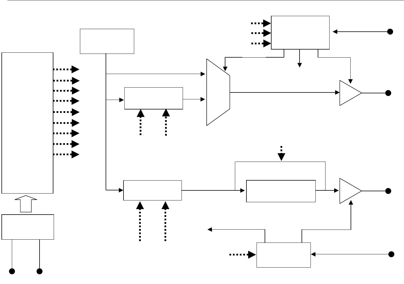
DESCRIPTION
The DS1077 is a dual-output, programmable, fixed-frequency oscillator requiring no external
components for operation. The DS1077 can be used as a processor-controlled frequency synthesizer or
as a standalone oscillator. The two synchronous output operating frequencies are user-adjustable in
submultiples of the master frequency through the use of two on-chip programmable prescalers and a
divider. The specific output frequencies chosen are stored in NV (EEPROM) memory. The DS1077
defaults to these values upon power-up.
The DS1077 features a 2-wire serial interface that allows in-circuit on-the-fly programming of the
programmable prescalers (P0 & P1) and divider (N) with the desired values being stored in NV
(EEPROM) memory. Design changes can be accommodated in-circuit on-the-fly by simply
programming different values into the device (or reprogramming previously programmed devices).
Alternatively, for fixed frequency applications, previously programmed devices can be used and no
connection to the serial interface is required. Pre-programmed devices can be ordered in customer-
requested frequencies.
The DS1077 is available in 8-pin SO or µSOP packages, allowing the generation of a clock signal
easily, economically, and using minimal board area. Chip-scale packaging is also available on request.
DS1077
EconOscillator/Divide
r
www.maxim-ic.com
150mil SO
118mil µSOP Package
V
CC
EconOscillator is a trademark of Dallas Semiconductor.
DS1077
2 of 21
BLOCK DIAGRAM 1077 Figure1
PROGRAMMABLE
“N” DIVIDER
CONTROL
LOGIC
(TABLE 1)
CONTROL
LOGIC
2-WIRE
INTERFACE
DIV1
0M1
0M0
1M1
1M0
EN0
SEL0
PDN0
PDN1
CONTROL
REGISTERS
SCL SDA
INTERNAL
OSCILLATOR
P0 PRESCALER
(M DIVIDER)
P1 PRESCALER
(
M DIVIDER
)
0M0 0M1
1M0 1M1
MUX
PDN0
EN0
SEL0
Power-Down
OUT0
CTRL0
Enable
Select
OUT1
DIV1
CTRL1
PDN1
(TABLE 2)
MCLK
Power-Down
Enable
DS1077
3 of 21
OVERVIEW
A block diagram of the DS1077 is shown in Figure 1. The DS1077 consists of four major components:
1) Internal Master Oscillator, 2) Prescalers, 3) Programmable Divider, and 4) Control Registers.
The internal oscillator is factory-trimmed to provide a master frequency (Master CLK) that can be routed
directly to the outputs (OUT0 & OUT1) or through separate prescalers (P0 & P1). OUT1 can also be
routed through an additional divider (N).
The Prescaler (P0) divides the Master Clock by 1, 2, 4, or 8 to be routed directly to the OUT0 pin.
The Prescaler (P1) divides the Master Clock by 1, 2, 4, or 8, which can be routed directly to the OUT1 pin
or to the Divider (N) input, which is then routed to the OUT1 pin.
The Programmable Divider (N) divides the Prescaler Output (P1) by any number selected between 2 and
1025 to provide the Main Output (OUT1) or it can be bypassed altogether by use of the DIV1 register bit.
The value of N is stored in the DIV register.
The Control Registers are user-programmable through a 2-wire serial interface to determine operating
frequency (values of P0, P1, & N) and modes of operation. The register values are stored in EEPROM
and therefore only need to be programmed to alter frequencies and operating modes.
PIN DESCRIPTIONS
Output 1 (OUT1)—This pin is the main oscillator output; its frequency is determined by the control
register settings for the prescaler P1 (mode bits 1M1 & 1M0) and divider N (DIV word).
Output 0 (OUT0)—A reference output, OUT0, is taken from the output of the reference select Mux. Its
frequency is determined by the control register settings for CTRL0 and values of Prescaler P0 (mode bits
0M1 & 0M0) (see Table 1).
Control Pin 0 (CTRL0)—A multifunctional input pin that can be selected as a MUX SELECT,
OUTPUT ENABLE and/or a POWER-DOWN. Its function is determined by the user-programmable
control register values EN0, SEL0, and PDN0 (see Table 1).
Control Pin 1 (CTRL1)—A multifunctional input pin that can be selected as a OUTPUT ENABLE
and/or a POWER-DOWN. Its function is determined by the user-programmable control register value of
PDN1 (see Table 2).
Serial Data Input/Output (SDA)—Input/Output pin for the 2-wire serial interface used for data transfer.
Serial Clock Input (SCL)—Input pin for the 2-wire serial interface used to synchronize data movement
on the serial interface.

DS1077U-120+

Mfr. #:
Manufacturer:
Maxim Integrated
Description:
Clock Generators & Support Products EconOscillator/Dvdr 120MHz 150mil 2-Wire
Lifecycle:
New from this manufacturer.
Delivery:
DHL FedEx Ups TNT EMS
Payment:
T/T Paypal Visa MoneyGram Western Union