DS1077
16 of 21
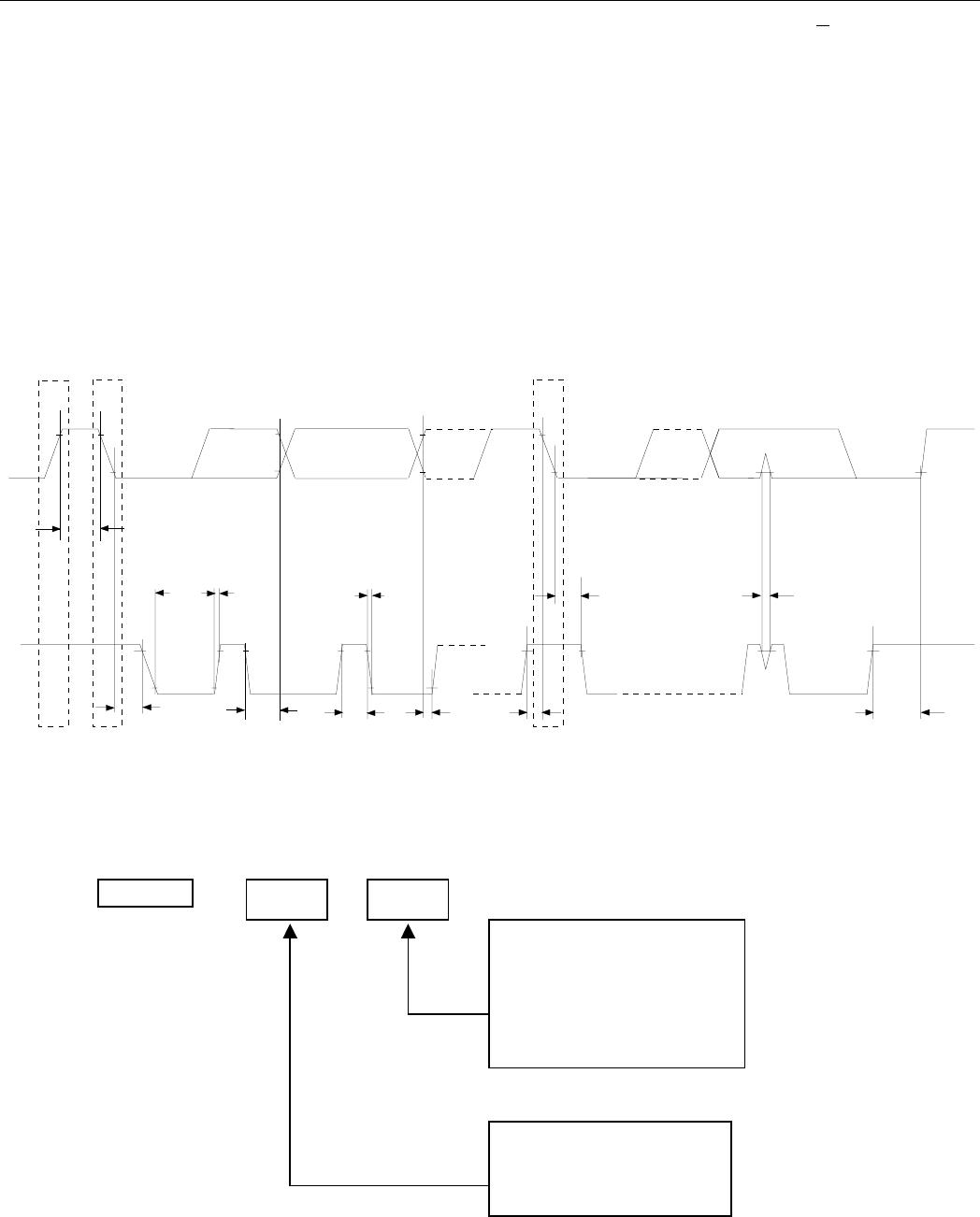
AC ELECTRICAL CHARACTERISTICS: 2-WIRE INTERFACE
(-40°C to +85°C; V
CC
= 5V±5%)
PARAMETER
SYMBOL
CONDITION
MIN
TYP
MAX
UNITS
NOTES
Fast Mode 400 SCL Clock Frequency f
SCL
Standard Mode 100
kHz
Fast Mode 1.3 Bus Free Time
Between a STOP
and START Condition
t
BUF
Standard Mode 4.7
µs
Fast Mode 0.6 Hold Time (Repeated)
START Condition
t
HD:STA
Standard Mode 4.0
µs 6
Fast Mode 1.3 LOW Period of SCL t
LOW
Standard Mode 4.7
µs
Fast Mode 0.6 HIGH Period of SCL t
HIGH
Standard Mode 4.0
µs
Fast Mode 0.6 Set-Up Time for a
Repeated START
t
SU:STA
Standard Mode 4.7
µs
Fast Mode 0 Data Hold Time t
HD:DAT
Standard Mode 0
0.9 µs 7,8
Fast Mode 100 Data Set-Up Time t
SU:DAT
Standard Mode 250
ns
Fast Mode 300 Rise Time of Both
SDA and SCL Signals
t
R
Standard Mode
20 + 0.1C
B
1000
ns 9
Fast Mode Fall Time of Both SDA
and SCL Signals
t
F
Standard Mode
20 + 0.1C
B
300 ns 9
Fast Mode 0.6 Set-Up Time For STOP t
SU:STO
Standard Mode 4.0
µs
Capacitive Load for
Each Bus Line
C
B
400 pF 9
Input Capacitance C
I
5 pF
NONVOLATILE MEMORY CHARACTERISTICS
PARAMETER SYMBOL CONDITION MIN TYP MAX UNITS NOTES
Writes +85°C 10,000
NOTES:
1) All voltages are referenced to ground.
2) 8.13kHz is obtained from a -66MHz standard part.
3) PDN is a power-down signal applied to either CTRL0 or CTRL1 pins as appropriate.
4) Output voltage swings may be impaired at high frequencies combined with high output loading.
5) After this period, the first clock pulse is generated.
6) A device must internally provide a hold time of at least 300ns for the SDA signal (referred to the V
IH
MIN
of the SCL signal) in order to bridge the undefined region of the falling edge of SCL.
7) The maximum t
HD:DAT
has only to be met if the device does not stretch the LOW period (t
LOW
) of the SCL
signal.
DS1077
17 of 21
8) A fast mode device can be used in a standard mode system, but the requirement t
SU:DAT
>250ns must then
be met. This will automatically be the case if the device does not stretch the LOW period of the SCL
signal. If such a device does stretch the LOW period of the SCL signal, it must output the next data bit to
the SDA line t
R MAX
+ t
SU:DAT
= 1000ns + 250ns = 1250ns before the SCL line is released.
9) C
B
is the total capacitance of one bus line in pF.
10) OUT0 and OUT1 are operating at oscillator master frequency without divider.
11) Typical frequency shift due to aging is ±0.5%. Aging stressing includes Level 3 preconditioning with
1000 temperature cycles of -55°C to +125°C, 336hr max V
CC
biased +125°C bake. Level 3
preconditioning consists of a 24hr +125°C storage bake, 192hr moisture soak at +30°C/60% R.H., and
three solder reflow passes.
TIMING DIAGRAM
SU:STO
t
t
SP
HD:STA
t
t
SU:STA
SU:DAT
t
t
HIGH
R
t
t
LOW
t
HD:STA
SCL
START
SDA
STOP
t
BUF
t
F
REPEATED
START
t
HD:DAT
ORDERING INFORMATION
Example:
DS1077Z-100
DS1077
Z = SO
U = µSOP
133 = 133.333MHz
125 = 125.000MHz
120 = 120.000MHz
100 = 100.000MHz
66 = 66.666MHz
DS1077
18 of 21
TYPICAL OPERATING CHARACTERISTICS
(V
CC
= 5.0V, T = +25°C, unless otherwise specified)
SUPPLY CURRENT vs. VOLTAGE
0.00
5.00
10.00
15.00
20.00
25.00
30.00
35.00
40.00
45.00
4.54.74.95.15.35.5
VOLTAGE (V)
CURRENT (mA)
DS1077-133
DS1077-100
DS1077-66
SUPPLY CURRENT vs. DIVISOR (N)
DS1077-133
20
22
24
26
28
30
32
34
0 200 400 600 800 1000
DIVISOR (N)
CURRENT (mA)
4.75V
5.0V
5.25V

DS1077U-120+

Mfr. #:
Manufacturer:
Maxim Integrated
Description:
Clock Generators & Support Products EconOscillator/Dvdr 120MHz 150mil 2-Wire
Lifecycle:
New from this manufacturer.
Delivery:
DHL FedEx Ups TNT EMS
Payment:
T/T Paypal Visa MoneyGram Western Union