BGA2803 All information provided in this document is subject to legal disclaimers. © NXP Semiconductors N.V. 2015. All rights reserved.
Product data sheet Rev. 5 — 13 July 2015 4 of 18
NXP Semiconductors
BGA2803
MMIC wideband amplifier
8. Application information
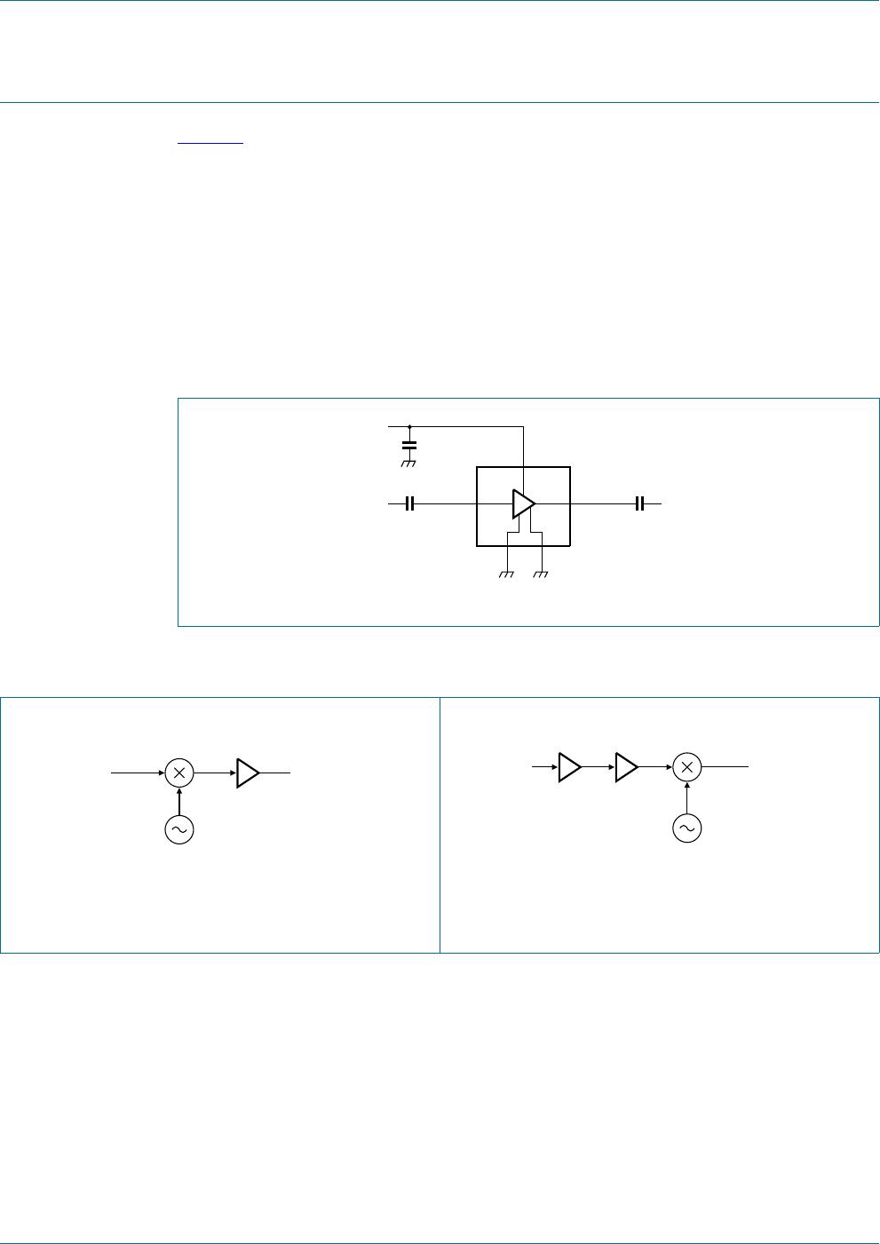
Figure 1 shows a typical application circuit for the BGA2803 MMIC. The device is
internally matched to 50 , and therefore does not need any external matching. The value
of the input and output DC blocking capacitors C2 and C3 should not be more than 100 pF
for applications above 100 MHz. However, when the device is operated below 100 MHz,
the capacitor value should be increased.
The location of the 470 pF supply decoupling capacitor (C
dec
) can be precisely chosen for
optimum performance.
The PCB top ground plane, connected to pins 2, 4 and 5 must be as close as possible to
the MMIC, preferably also below the MMIC. When using via holes, use multiple via holes
as close as possible to the MMIC.
8.1 Application examples
Fig 1. Typical application circuit
The MMIC is very suitable as IF amplifier in e.g. LNB’s.
The excellent wideband characteristics make it an easy
building block.
As second amplifier after an LNA, the MMIC offers an
easy matching, low noise solution.
Fig 2. Application as IF amplifier Fig 3. Application as RF amplifier
DDI
IURP5)
FLUFXLW
RVFLOODWRU
ZLGHEDQG
DPSOLILHU
WR,)FLUFXLW
RUGHPRGXODWRU
PL[HU
DDI
DQWHQQD
RVFLOODWRU
ZLGHEDQG
DPSOLILHU
/1$
WR,)FLUFXLW
RUGHPRGXODWRU
PL[HU