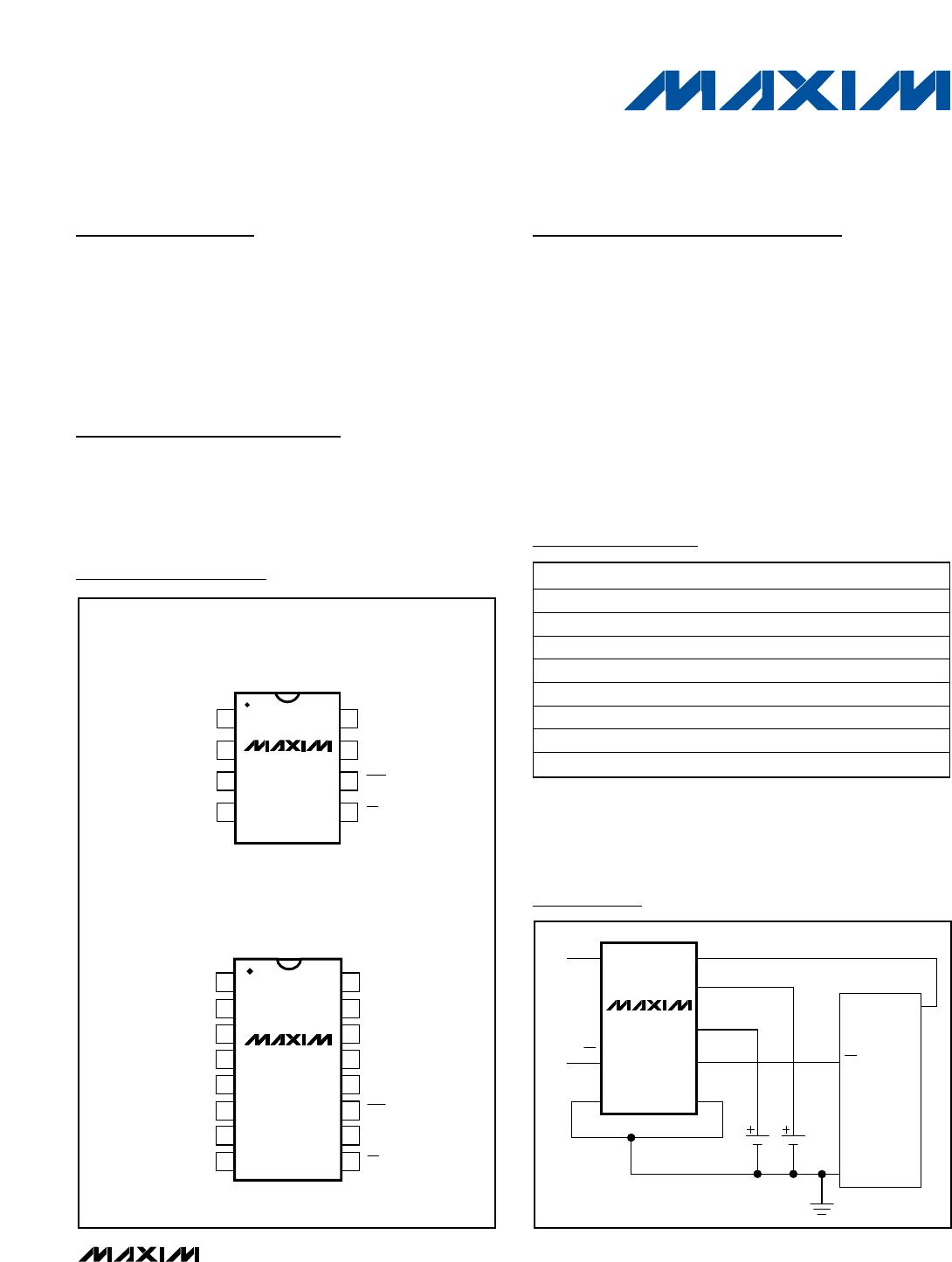
MXD1210CPA

General Description
The MXD1210 nonvolatile RAM controller is a very low-
power CMOS circuit that converts standard (volatile)
CMOS RAM into nonvolatile memory. It also continually
monitors the power supply to provide RAM write protec-
tion when power to the RAM is in a marginal (out-of-tol-
erance) condition. When the power supply begins to
fail, the RAM is write-protected, and the device switch-
es to battery-backup mode.
Applications
Microprocessor Systems
Computers
Embedded Systems
Features
Battery Backup
Memory Write Protection
230µA Operating Mode Quiescent Current
2nA Backup Mode Quiescent Current
Battery Freshness Seal
Optional Redundant Battery
Low Forward-Voltage Drop on V
CC
Supply Switch
5% or 10% Power-Fail Detection Options
Tests Battery Condition During Power-Up
8-Pin SO Available
MXD1210
Nonvolatile RAM Controller
________________________________________________________________
Maxim Integrated Products
1
8
V
CCI
+5V
1
2
7
VBATT2
6
3
5
4
GND
CE
V
CC
CMOS
RAM
MXD1210
CE
FROM
DECODER
VBATT1
V
CCO
PART TEMP RANGE PIN-PACKAGE
MXD1210C/D 0°C to +70°C Dice*
MXD1210CPA 0°C to +70°C 8 PDIP
MXD1210CSA 0°C to +70°C 8 SO
MXD1210CWE 0°C to +70°C 16 Wide SO
MXD1210EPA -40°C to +85°C 8 PDIP
MXD1210ESA -40°C to +85°C 8 SO
MXD1210EWE -40°C to +85°C 16 Wide SO
MXD1210MJA -55°C to +125°C 8 CERDIP
Typical Operating Circuit
Ordering Information
CEO
CEGND
1
2
8
7
V
CCI
VBATT2VBATT1
TOL
V
CCO
DIP/SO
TOP VIEW
3
4
6
5
MXD1210
16
15
14
13
12
11
10
9
1
2
3
4
5
6
7
8
N.C.
N.C.
V
CCI
N.C.
VBATT2
N.C.
CEO
N.C.
CE
MXD1210
WIDE SO
V
CCO
N.C.
TOL
VBATT1
N.C.
N.C.
GND
Pin Configurations
19-0154; Rev 2; 11/05
For pricing, delivery, and ordering information, please contact Maxim/Dallas Direct! at
1-888-629-4642, or visit Maxim’s website at www.maxim-ic.com.
*
Contact factory for dice specifications.
Devices in PDIP and SO packages are available in both lead-
ed and lead-free packaging. Specify lead free by adding the +
symbol at the end of the part number when ordering. Lead free
not available for CERDIP package.
MXD1210
Nonvolatile RAM Controller
2 _______________________________________________________________________________________
ABSOLUTE MAXIMUM RATINGS
RECOMMENDED OPERATING CONDITIONS
(T
A
= T
MIN
to T
MAX
, unless otherwise noted.)
Stresses beyond those listed under “Absolute Maximum Ratings” may cause permanent damage to the device. These are stress ratings only, and functional
operation of the device at these or any other conditions beyond those indicated in the operational sections of the specifications is not implied. Exposure to
absolute maximum rating conditions for extended periods may affect device reliability.
V
CCI
to GND ..........................................................-0.3V to +7.0V
VBATT1 to GND.....................................................-0.3V to +7.0V
VBATT2 to GND.....................................................-0.3V to +7.0V
V
CCO
to GND ................................................-0.3V to (V
S
+ 0.3V)
(V
S
= greater of V
CCI
, VBATT1, VBATT2)
Digital Input and Output
Voltages to GND.....................................-0.3V to (V
CCI
+ 0.3V)
Continuous Power Dissipation (T
A
= +70°C)
8-Pin PDIP (derate 9.09mW/°C above +70°C)..............727mW
8-Pin SO (derate 5.88mW/°C above +70°C).................471mW
8-Pin CERDIP (derate 8.00mW/°C above +70°C).........640mW
16-Pin Wide SO (derate 9.52mW/°C above +70°C) .....762mW
Operating Temperature Range
C Suffix.................................................................0°C to +70°C
E Suffix..............................................................-40°C to +85°C
M Suffix ...........................................................-55°C to +125°C
Storage Temperature Range .............................-65°C to +150°C
Lead Temperature (soldering, 10s) .................................+300°C
PARAMETER SYMBOL CONDITIONS MIN TYP MAX UNITS
TOL = GND 4.75 5.50
Supply Voltage V
CCI
TOL = V
CCO
4.50 5.50
V
Input High Voltage V
IH
2.2 V
Input Low Voltage V
IL
0.8 V
Battery Voltage
VBATT1
VBATT2
1 or 2 batteries (Note 1) 2.0 4.0 V
ELECTRICAL CHARACTERISTICS—Normal Supply Mode, TOL = V
CCO
(V
CCI
= +4.75V to +5.5V, TOL = GND; or V
CCI
= +4.5V to +5.5V, TOL = V
CCO
; T
A
= T
MIN
to T
MAX
, unless otherwise noted.)
PARAMETER SYMBOL CONDITIONS MIN TYP MAX UNITS
Supply Current I
CCI
V
CCO
, CEO open, VBATT1 = VBATT2 = 3V 0.23 0.5 mA
MXD1210C
V
CCI
-
0.20
MXD1210E
V
CCI
-
0.21
Output Supply Voltage V
CCO
I
CCO1
= 80mA (Note 2)
MXD1210M
V
CCI
-
0.25
V
MXD1210C 80
MXD1210E 0.23 75
Output Supply Current I
CCO
V
CCI
- V
CCO
0.2V (Note 2)
MXD1210M 0.23 65
mA
Input Leakage Current I
IL
±1.0 µA
Output Leakage Current I
OL
±1.0 µA
High-Level Output Voltage V
OH
I
OH
= -1mA 2.4 V
Low-Level Output Voltage V
OL
I
OL
= 4mA 0.4 V
TOL = GND 4.50 4.74
V
CCI
Trip Point V
CCTP
TOL = V
CCO
4.25 4.49
V
MXD1210
Nonvolatile RAM Controller
_______________________________________________________________________________________ 3
Note 1: Only one battery input is required. Unused battery inputs must be grounded.
Note 2: I
CCO1
is the maximum average load current the MXD1210 can supply to the memories.
Note 3: I
CCO2
is the maximum average load current the MXD1210 can supply to the memories in battery-backup mode.
Note 4: CEO can sustain leakage current only in battery-backup mode.
Note 5: Guaranteed by design.
Note 6: t
CE
max must be met to ensure data integrity on power loss.
ELECTRICAL CHARACTERISTICS—Battery-Backup Mode
(V
CCI
< V
BATT
, positive edge rate at VBATT1, VBATT2 > 0.1V/µs, T
A
= T
MIN
to T
MAX
, unless otherwise noted.)
PARAMETER SYMBOL CONDITIONS MIN TYP MAX UNITS
MXD1210C/E 2 100 nA
Quiescent Current (Note 1) I
BATT
V
CCO
, CEO open,
V
CCI
= 0V
MXD1210M 5 µA
Output Supply Current I
CCO2
V
BATT
- V
CCO
0.2V (Notes 3, 4) 300 µA
CEO Output Voltage V
O
Output open
V
BATT
-
0.2
V
CAPACITANCE
(T
A
= T
MIN
to T
MAX
, unless otherwise noted.) (Note 5)
PARAMETER SYMBOL CONDITIONS MIN TYP MAX UNITS
Input Capacitance C
IN
5pF
Output Capacitance C
OUT
7pF
V
CC
POWER TIMING CHARACTERISTICS
(V
CCI
= +4.75V to +5.5V, TOL = GND; or V
CCI
= +4.5V to +5.5V, TOL = V
CCO
, T
A
= T
MIN
to T
MAX
, unless otherwise noted.)
PARAMETER SYMBOL CONDITIONS MIN TYP MAX UNITS
MXD1210C 5 10 20
MXD1210E 5 10 22
CE Propagation Delay t
PD
R
L
= 1kΩ, C
L
= 50pF
MXD1210M 5 10 25
ns
CE High to Power-Fail t
PF
(Note 5) 0 ns
TIMING CHARACTERISTICS
(V
CCI
< +4.75V to +5.5V, TOL = GND; or V
CCI
< +4.5V, TOL = V
CCO
, T
A
= T
MIN
to T
MAX
, unless otherwise noted.)
PARAMETER SYMBOL CONDITIONS MIN TYP MAX UNITS
Recovery at Power-Up t
REC
2520ms
t
F
To out-of-tolerance condition 300
V
CC
Slew-Rate Power-Down
t
FB
Tolerance to battery power 10
µs
V
CC
Slew-Rate Power-Up t
R
s
CE Pulse Width t
CE
(Note 6) 1.5 µs

MXD1210CPA

Mfr. #:
Manufacturer:
Maxim Integrated
Description:
Supervisory Circuits Nonvolatile RAM Controller
Lifecycle:
New from this manufacturer.
Delivery:
DHL FedEx Ups TNT EMS
Payment:
T/T Paypal Visa MoneyGram Western Union