MXD1210
Nonvolatile RAM Controller
_______________________________________________________________________________________ 5_______________________________________________________________________________________ 5
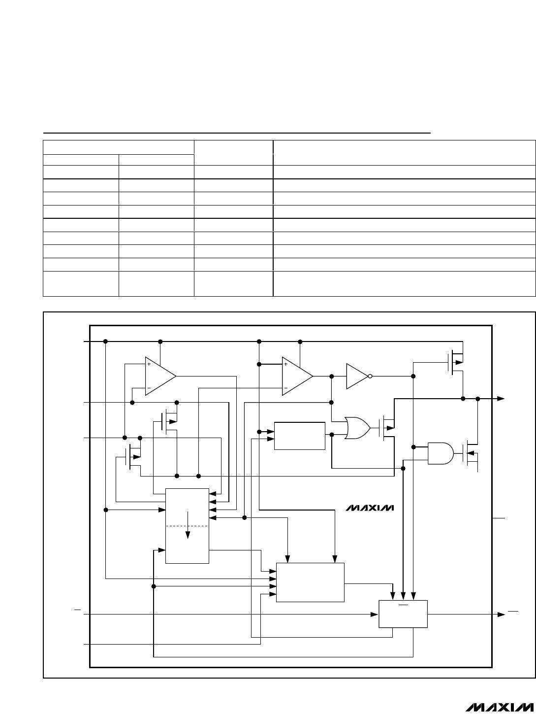
Detailed Description
Main Functions
The MXD1210 executes five main functions to perform
reliable RAM operation and battery backup (see the
Typical Operating Circuit
and Figure 1):
1) RAM Power-Supply Switch: The switch directs
power to the RAM from the incoming supply or
from the selected battery, whichever is at the
greater voltage. The switch control uses the same
criterion to direct power to MXD1210 internal cir-
cuitry.
2) Power-Failure Detection: The write-protection
function is enabled when a power failure is
detected. The power-failure detection range
depends on the state of the TOL pin as follows:
Power-failure detection is independent of the bat-
tery-backup function and precedes it sequentially
as the power-supply voltage drops during a typi-
cal power failure.
3) Write Protection: This holds the chip-enable out-
put (CEO) to within 0.2V of V
CCI
or of the selected
battery, whichever is greater. If the chip-enable
input (CE) is low (active) when power failure is
detected, then CEO is held low until CE is brought
high, at which time CEO is gated high for the
duration of the power failure. The preceding
sequence completes the current RD/WR cycle,
preventing data corruption if the RAM access is a
WR cycle.
4) Battery Redundancy: A second battery is option-
al. When two batteries are connected, the
stronger battery is selected to provide RAM back-
up and to power the MXD1210. The battery-selec-
tion circuitry remains active while in the
battery-backup mode, selecting the stronger bat-
tery and isolating the weaker one. The battery-
selection activity is transparent to the user and
the system. If only one battery is connected, the
second battery input should be grounded.
5) Battery-Status Warning: This notifies the system
when the stronger of the two batteries measures ≤
2.0V. Each time the MXD1210 is repowered (V
CCI
> V
CCTP
) after detecting a power failure, the bat-
tery voltage is measured. If the battery in use is
low, following the MXD1210 recovery period, the
device issues a warning to the system by inhibit-
ing the second memory cycle. The sequence is
as follows:
First access: read memory location n, loc(n) = x
Second access: write memory location n,
loc(n) = complement (x)
Third access: read memory location n, loc(n) = ?
If the third access (read) is complement (x), then the
battery is good; otherwise the battery is not good.
Return to loc(n) = x following the test sequence.
Freshness-Seal Mode
The freshness-seal mode relates to battery longevity
during storage rather than directly to battery backup.
This mode is activated when the first battery is con-
nected, and is defeated when the voltage at V
CCI
first
exceeds V
CCTP
. In the freshness-seal mode, both bat-
teries are isolated from the system; that is, no current is
drained from either battery, and the RAM is not pow-
ered by either battery. This means that batteries can be
installed and the system can be held in inventory with-
out battery discharge. The positive edge rate at
VBATT1 and VBATT2 should exceed 0.1V/µs. The bat-
teries will maintain their full shelf life while installed in
the system.
Battery Backup
The
Typical Operating Circuit
shows the MXD1210 con-
nected to write-protect the RAM when V
CC
is less than
4.75V, and to provide battery backup to the supply.