74LVC2G66
Bilateral switch
Rev. 10 — 13 April 2017 Product data sheet
1 General description
The 74LVC2G66 is a low-power, low-voltage, high-speed Si-gate CMOS device.
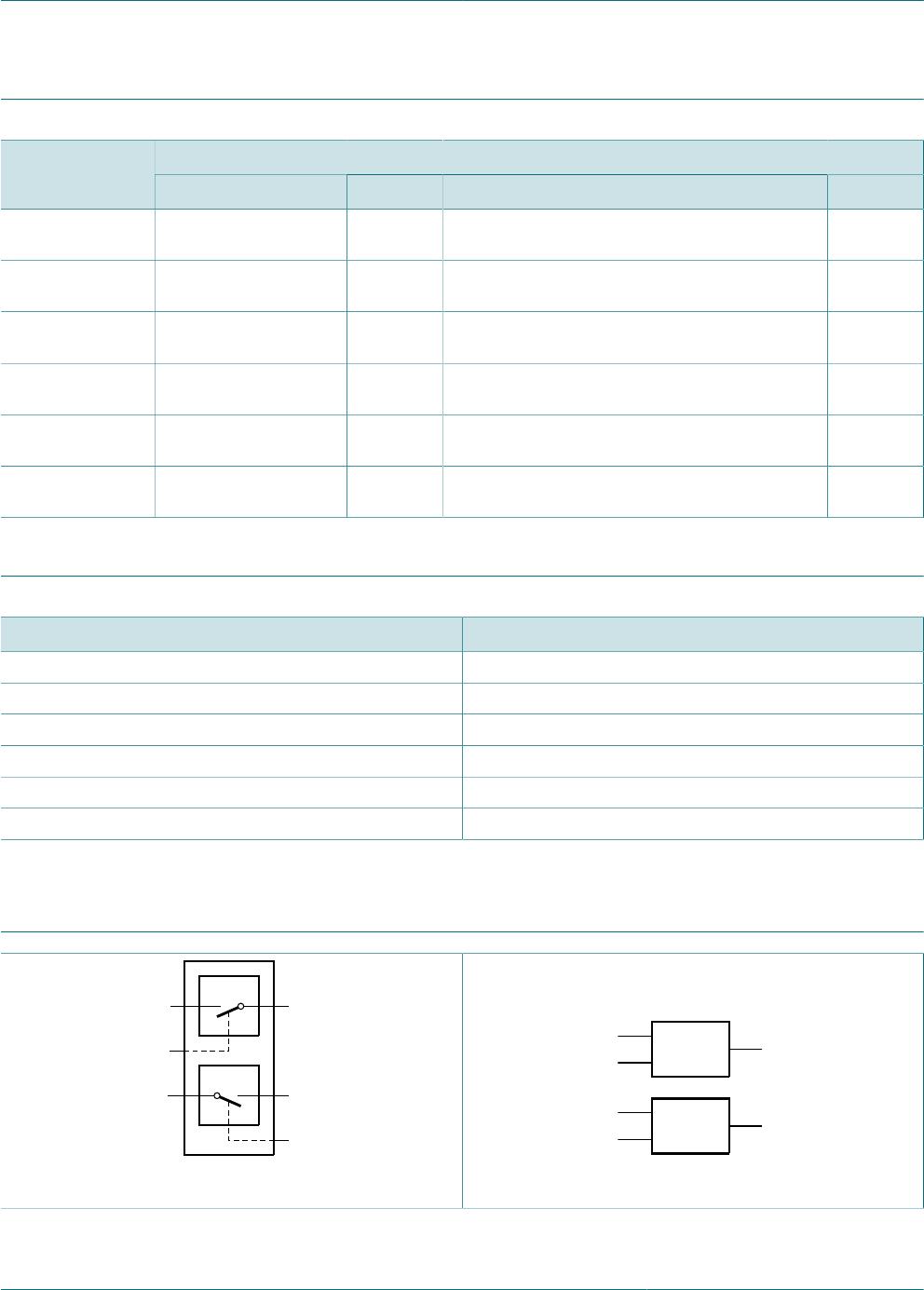
The 74LVC2G66 provides two single pole, single-throw analog switch functions. Each
switch has two input/output terminals (nY and nZ) and an active HIGH enable input (nE).
When nE is LOW, the analog switch is turned off.
Schmitt trigger action at the enable inputs makes the circuit tolerant of slower input rise
and fall times across the entire V
CC
range from 1.65 V to 5.5 V.
2 Features and benefits
• Wide supply voltage range from 1.65 V to 5.5 V
• Very low ON resistance:
– 7.5 Ω (typical) at V
CC
= 2.7 V
– 6.5 Ω (typical) at V
CC
= 3.3 V
– 6 Ω (typical) at V
CC
= 5 V
• Switch current capability of 32 mA
• High noise immunity
• CMOS low power consumption
• TTL interface compatibility at 3.3 V
• Latch-up performance meets requirements of JESD78 Class I
• ESD protection:
– HBM JESD22-A114F exceeds 2000 V
– MM JESD22-A115-A exceeds 200 V
• Enable input accepts voltages up to 5.5 V
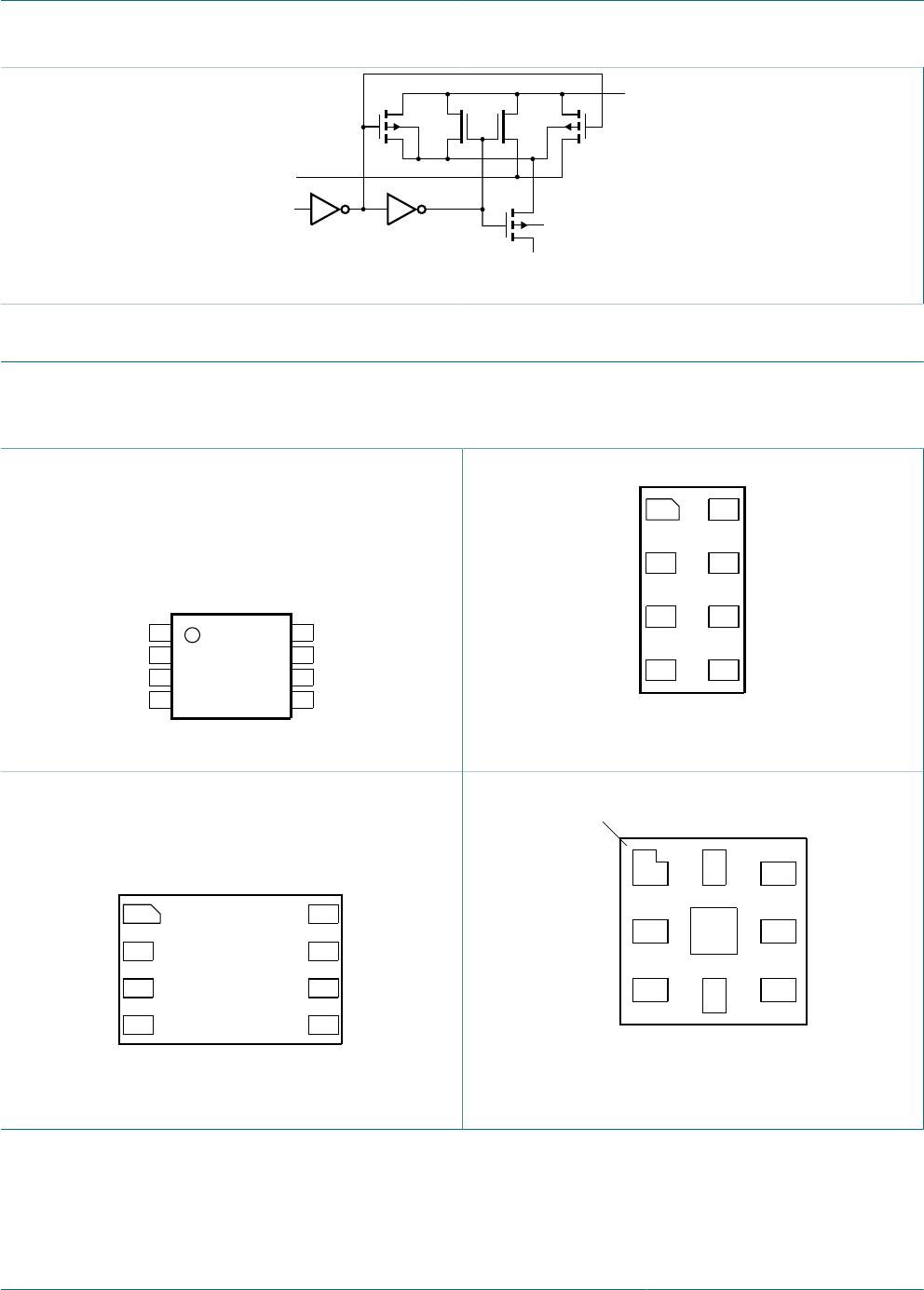
• Multiple package options
• Specified from -40 °C to +85 °C and -40 °C to +125 °C