AD8314
Rev. B | Page 12 of 20
APPLICATIONS
BASIC CONNECTIONS
Figure 31 shows connections for the basic measurement mode.
A supply voltage of 2.7 V to 5.5 V is required. The supply to the
VPOS pin should be decoupled with a low inductance 0.1 µF
surface-mount ceramic capacitor. A series resistor of about 10 Ω
can be added; this resistor slightly reduces the supply voltage to the
AD8314 (maximum current into the VPOS pin is approximately
9 mA when V_DN is delivering 5 mA). Its use should be
avoided in applications where the power supply voltage is very
low (that is, 2.7 V). A series inductor provides similar power
supply filtering with minimal drop in supply voltage.
C
F
OPTIONAL
(SEE TEXT)
0.1µ
F
OPTIONAL
(SEE TEXT)
V
S
V
S
V
DN
V
UP
INPUT
1
2
3
4
ENBL
RFIN
AD8314
8
7
6
5
VSET
FLTR
V_DN
VPOS
COMM
V_UP
52.3
01086-031
Figure 31. Basic Connections for Operation in Measurement Mode
The ENBL pin is here connected to VPOS. The AD8314 can be
disabled by pulling this pin to ground when the chip current is
reduced to about 20 µA from its normal value of 4.5 mA. The
logic threshold is around +V
S
/2 and the enable function occurs
in about 1.5 µs. Note, however, further settling time is generally
needed at low input levels.
The AD8314 has an internal input coupling capacitor. This
eliminates the need for external ac coupling. A broadband input
match is achieved in this example by connecting a 52.3 Ω resistor
between RFIN and ground. This resistance combines with the
internal input impedance of approximately 3 kΩ to give an
overall broadband input resistance of 50 Ω. Several other
coupling methods are possible, which are described in the
Input Coupling Options section.
The measurement mode is selected by connecting VSET to
V_UP, which establishes a feedback path and sets the
logarithmic slope to its nominal value. The peak voltage range
of the measurement extends from −58 dBV to −13 dBV at
0.9 GHz, and only slightly less at higher frequencies up to
2.5 GHz. Therefore, using the 50 Ω termination, the equivalent
power range is −45 dBm to 0 dBm. At a slope of 21.5 mV/dB,
this would amount to an output span of 967 mV.
Figure 32
shows the transfer function for V_UP at a supply voltage of 3 V
and input frequency of 0.9 GHz.
V_DN, which is generally not used when the AD8314 is used in
measurement mode, is essentially an inverted version of V_UP.
The voltage on V_UP and V_DN are related by
V
DN
= 2.25 V − 2 V
UP
While V_DN can deliver up to 6 mA, the load resistance on
V_UP should not be lower than 10 kΩ in order that the full-
scale output of 1 V can be generated with the limited available
current of 200 µA maximum.
Figure 32 shows the logarithmic
conformance under the same conditions.
1.2
0
–70 0
INPUT AMPLITUDE (dBV)
V
UP
(V)
ERROR (dB)
3
–3
–2
–1
0
1
2
1.0
0.8
0.6
0.4
0.2
–60 –50 –40 –30 –20 –10
V
S
= 3V
R
T
= 52.3
±1dB DYNAMIC RANGE
±3dB DYNAMIC RANGE
INTERCEPT
(–47dBm) (+3dBm)
01086-032
Figure 32. V
UP
and Log Conformance Error vs.
Input Level vs. Input Level at 900 MHz
TRANSFER FUNCTION IN TERMS OF SLOPE AND
INTERCEPT
The transfer function of the AD8314 is characterized in terms
of its slope and intercept. The logarithmic slope is defined as the
change in the RSSI output voltage for a 1 dB change at the input.
For the AD8314, slope is nominally 21.5 mV/dB. Therefore, a
10 dB change at the input results in a change at the output of
approximately 215 mV. Log conformance plot,
Figure 32, shows
the range over which the device maintains its constant slope.
The dynamic range can be defined as the range over which the
error remains within a certain band, usually ±1 dB or ±3 dB. In
Figure 32 for example, the ±1 dB dynamic range is approximately
50 dB (from −13 dBV to −63 dBV).
AD8314
Rev. B | Page 13 of 20
The intercept is the point at which the extrapolated linear
response would intersect the horizontal axis (see
Figure 32).
Using the slope and intercept, the output voltage can be
calculated for any input level within the specified input range by
V
UP
= V
SLOPE
× (P
IN
P
O
)
where:
V
UP
is the demodulated and filtered RSSI output.
V
SLOPE
is the logarithmic slope, expressed in V/dB.
P
IN
is the input signal, expressed in decibels relative to some
reference level (either dBm or dBV in this case).
P
O
is the logarithmic intercept, expressed in decibels relative to
the same reference level.
For example, at an input level of −40 dBV (−27 dBm), the
output voltage is
V
OUT
= 0.020 V/dB × [−40 dBV − (−63 dBV)] = 0.46 V
dBV VS. dBm
The most widely used convention in RF systems is to specify
power in dBm, that is, decibels above 1 mW in 50 Ω. Specification
of log amp input levels in terms of power is strictly a concession
to popular convention; they do not respond to power (tacitly
power absorbed at the input), but to the input voltage. The use
of dBV, defined as decibels with respect to a 1 V rms sine wave,
is more precise, although this is still not unambiguous because
waveform is also involved in the response of a log amp, which,
for a complex input (such as a CDMA signal), does not follow
the rms value exactly. Since most users specify RF signals in
terms of power (more specifically, in dBm/50 Ω), both dBV and
dBm are used in specifying the performance of the AD8314
showing equivalent dBm levels for the special case of a
50 Ω environment. Values in dBV are converted to
dBm re 50 Ω by adding 13.
FILTER CAPACITOR
The video bandwidth of both V_UP and V_DN is
approximately 3.5 MHz. In CW applications where the input
frequency is much higher than this, no further filtering of the
demodulated signal is required. Where there is a low frequency
modulation of the carrier amplitude, however, the low-pass
corner must be reduced by the addition of an external filter
capacitor, C
F
(see Figure 31). The video bandwidth is related
to C
F
by
()
F
C
BandwidthVideo
+××
=
pF5.3k13π2
1
OPERATING IN CONTROLLER MODE
Figure 33 shows the basic connections for operation in the
controller mode, and
Figure 34 shows a block diagram of a
typical controller mode application. The feedback from V_UP
to VSET is broken and the desired setpoint voltage is applied to
VSET from the controlling source (often this is a DAC). V
DN
rails high (2.2 V on a 3.3 V supply, and 1.9 V on a 2.7 V supply)
when the applied power is less than the value corresponding to
the setpoint voltage. When the input power slightly exceeds this
value, V
DN
would, in the absence of the loop via the power
amplifier gain pin, decrease rapidly toward ground. In the
closed loop, however, the reduction in V
DN
causes the power
amplifier to reduce its output. This restores a balance between
the actual power level sensed at the input of the AD8314 and
the demanded value determined by the setpoint. This assumes
that the gain control sense of the variable gain element is
positive, that is, an increasing voltage from V_DN tends to
increase gain. The output swing and current sourcing capability
of V_DN are shown in
Figure 22 and Figure 25.
0.1µ
F
V
S
V
S
V
DN
INPUT
VSET
1
2
3
4
ENBL
RFIN
AD8314
8
7
6
5
VSET
FLTR
V_DN
VPOS
COMM
V_UP
52.3
C
F
01086-033
Figure 33. Basic Connections for Operation in Controller Mode
DAC
FLTR
V_UP
VSET
AD8314
DIRECTIONAL
COUPLER
POWER
AMPLIFIER
RF INPUT
GAIN
CONTROL
VOLTAGE
RFIN
V_DN
C
F
52.3
01086-034
Figure 34. Typical Controller Mode Application
The relationship between the input level and the setpoint
voltage follows from the nominal transfer function of the device
(V
UP
vs. input amplitude, see Figure 4). For example, a voltage of
1 V on VSET demands a power level of 0 dBm at RFIN. The
corresponding power level at the output of the power amplifier
is greater than this amount due to the attenuation through the
directional coupler.
AD8314
Rev. B | Page 14 of 20
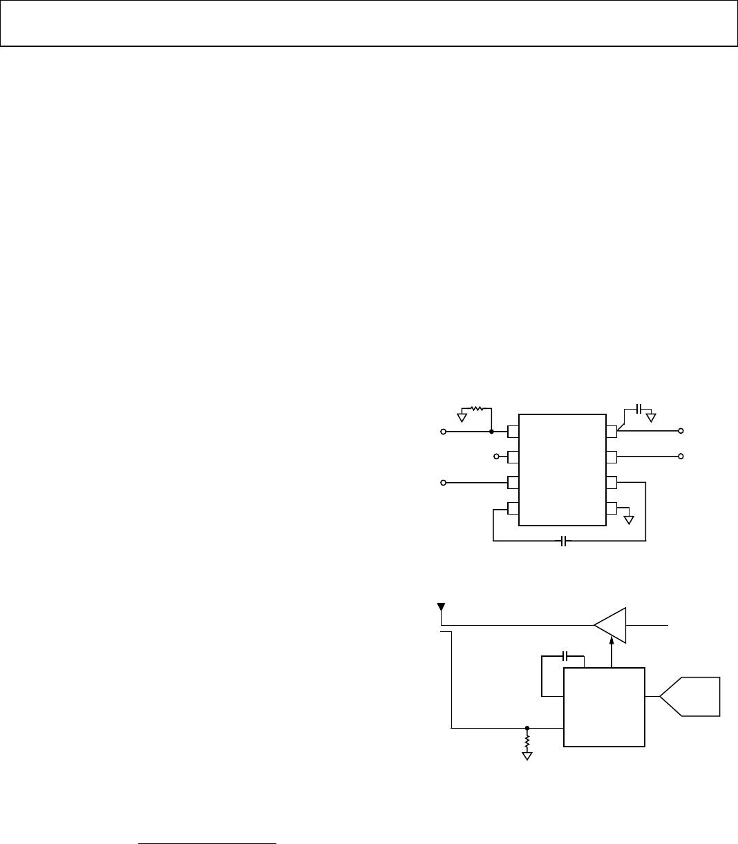
When connected in a PA control loop, as shown in Figure 34,
the voltage V
UP
is not explicitly used but is implicated in again
setting up the required averaging time, by choice of C
F
.
However, now the effective loop response time is a much more
complicated function of the PAs gain-control characteristics,
which are very nonlinear. A complete solution requires specific
knowledge of the power amplifier.
The transient response of this control loop is determined by the
filter capacitor, C
F.
When this is large, the loop is unconditionally
stable (by virtue of the dominant pole generated by this
capacitor), but the response is sluggish. The minimum value
ensuring stability should be used, requiring full attention to the
particulars of the power amplifier control function. Because this
is invariably nonlinear, the choice must be made for the worst-
case condition, which usually corresponds to the smallest
output from the PA, where the gain function is steepest. In
practice, an improvement in loop dynamics can often be
achieved by adding a response zero, formed by a resistor in
series with C
F
.
POWER-ON AND ENABLE GLITCH
As previously mentioned, the AD8314 can be put into a low
power mode by pulling the ENBL pin to ground. This reduces
the quiescent current from 4.5 mA to 20 µA. Alternatively, the
supply can be turned off to eliminate the quiescent current.
Figure 16 and Figure 26 show the behavior of the V_DN output
under these two conditions (in
Figure 26, ENBL is tied to
VPOS). The glitch that results in both cases can be reduced by
loading the V_DN output.
INPUT COUPLING OPTIONS
The internal 5 pF coupling capacitor of the AD8314, along with
the low frequency input impedance of 3 kΩ, gives a high-pass
input corner frequency of approximately 16 MHz. This sets the
minimum operating frequency.
Figure 35 through Figure 37
show three options for input coupling. A broadband resistive
match can be implemented by connecting a shunt resistor to
ground at RFIN (see
Figure 35). This 52.3 Ω resistor (other
values can also be used to select different overall input
impedances) combines with the input impedance of the
AD8314 (3 kΩ||2 pF) to give a broadband input impedance of
50 Ω. While the input resistance and capacitance (CIN and
RIN) varies by approximately ±20% from device to device, the
dominance of the external shunt resistor means that the variation
in the overall input impedance is close to the tolerance of the
external resistor.
At frequencies above 2 GHz, the input impedance drops below
250 Ω (see
Figure 12), so it is appropriate to use a larger value
shunt resistor. This value is calculated by plotting the input
impedance (resistance and capacitance) on a Smith Chart and
choosing the best value shunt resistor to bring the input
impedance closest to the center of the chart. At 2.5 GHz, a
shunt resistor of 165 Ω is recommended.
A reactive match can also be implemented as shown in
Figure 36.
This is not recommended at low frequencies as device
tolerances dramatically varies the quality of the match because
of the large input resistance. For low frequencies,
Figure 35 or
Figure 37 is recommended.
In
Figure 36, the matching components are drawn as general
reactances. Depending on the frequency, the input impedance at
that frequency, and the availability of standard value components,
either a capacitor or an inductor is used. As in the previous
case, the input impedance at a particular frequency is plotted on
a Smith Chart and matching components are chosen (shunt or
Series L, shunt or Series C) to move the impedance to the center
of the chart.
Table 5 gives standard component values for some
popular frequencies. Matching components for other frequencies
can be calculated using the input resistance and reactance data
over frequency, which is given in
Figure 12. Note that the
reactance is plotted as though it appears in parallel with the
input impedance (which it does because the reactance is
primarily due to input capacitance).
The impedance matching characteristics of a reactive matching
network provide voltage gain ahead of the AD8314; this increases
the device sensitivity (see
Table 5). The voltage gain is calculated by
1
2
log20
10
R
R
GainVoltage
dB
=
where R2 is the input impedance of the AD8314, and R1 is the
source impedance to which the AD8314 is being matched. Note
that this gain is only achieved for a perfect match. Component
tolerances and the use of standard values tend to reduce gain.
50 SOURCE
R
SHUNT
52.3
50
C
IN
R
IN
C
C
AD8314
RFIN
V
BIAS
01086-035
Figure 35. Broadband Resistive
50 SOURCE
X2
X1
50
C
IN
R
IN
C
C
AD8314
RFIN
V
BIAS
01086-036
Figure 36. Narrowband Reactive
STRIPLINE
C
IN
R
IN
C
C
AD8314
RFIN
V
BIAS
50
R
ATTN
01086-037
Figure 37. Series Attenuation

AD8314ARM-REEL7

Mfr. #:
Manufacturer:
Analog Devices Inc.
Description:
RF Detector RF Detector/Cntlr 100MHz-2.7GHz 45dB
Lifecycle:
New from this manufacturer.
Delivery:
DHL FedEx Ups TNT EMS
Payment:
T/T Paypal Visa MoneyGram Western Union