TLP3073,TLP3073F
4
7.
7.
7.
7. Absolute Maximum Ratings (Note) (Unless otherwise specified, T
Absolute Maximum Ratings (Note) (Unless otherwise specified, T
Absolute Maximum Ratings (Note) (Unless otherwise specified, T
Absolute Maximum Ratings (Note) (Unless otherwise specified, T
a
a
a
a
= 25
= 25
= 25
= 25
)
)
)
)
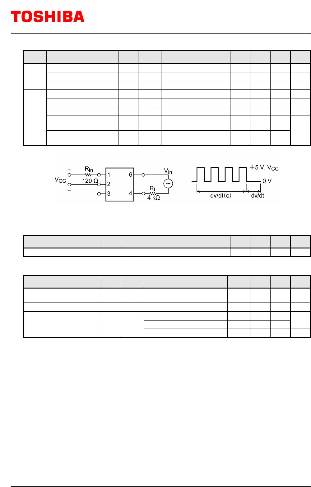
LED
Detector
Common
Characteristics
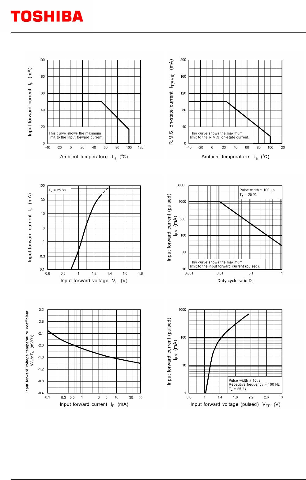
Input forward current
Input forward current derating
Input forward current (pulsed)
Input reverse voltage
Input power dissipation
Input power dissipation derating
Junction temperature
Off-state output terminal voltage
R.M.S. on-state current
R.M.S. on-state current derating
ON-state current (pulsed)
Peak non-repetitive surge current
Output power dissipation
Output power dissipation derating
Junction temperature
Total power dissipation
Total power dissipation derating
Operating temperature
Storage temperature
Lead soldering temperature
Isolation voltage
(T
a
≥ 53 )
(T
a
≥ 25 )
(T
a
= 25 )
(T
a
= 70 )
(T
a
≥ 25 )
(T
a
≥ 25 )
(T
a
≥ 25 )
(10 s)
AC, 60 s, R.H. ≤ 60 %
Symbol
I
F
∆I
F
/∆T
a
I
FP
V
R
P
D
∆P
D
/∆T
a
T
j
V
DRM
I
T(RMS)
∆I
T(RMS)
/∆T
a
I
ONP
I
TSM
P
O
∆P
O
/∆T
a
T
j
P
T
∆P
T
/∆T
a
T
opr
T
stg
T
sol
BV
S
Note
(Note 1)
(Note 2)
(Note 3)
(Note 4)
Rating
50
-0.7
1
5
100
-1.0
125
800
100
50
-1.1
2
1.2
300
-4.0
125
400
-4.4
-40 to 100
-55 to 125
260
5000
Unit
mA
mA/
A
V
mW
mW/
V
mA
mA
mA/
A
A
mW
mW/
mW
mW/
Vrms
Note: Using continuously under heavy loads (e.g. the application of high temperature/current/voltage and the
significant change in temperature, etc.) may cause this product to decrease in the reliability significantly even
if the operating conditions (i.e. operating temperature/current/voltage, etc.) are within the absolute maximum
ratings.
Please design the appropriate reliability upon reviewing the Toshiba Semiconductor Reliability Handbook
("Handling Precautions"/"Derating Concept and Methods") and individual reliability data (i.e. reliability test
report and estimated failure rate, etc).
Note 1: Pulse width (PW) ≤ 100 µs, 100 pps
Note 2: Pulse width (PW) ≤ 100 µs, 120 pps
Note 3: Pulse width (PW) ≤ 10 ms
Note 4: This device is considered as a two-terminal device: Pins 1, 2 and 3 are shorted together, and pins 4 and 6 are
shorted together.
8.
8.
8.
8. Recommended Operating Conditions (Note)
Recommended Operating Conditions (Note)
Recommended Operating Conditions (Note)
Recommended Operating Conditions (Note)
Characteristics
AC mains voltage
Input forward current
ON-state current (pulsed)
Operating temperature
Symbol
V
AC
I
F
I
ONP
T
opr
Note
(Note 1)
Min
7.5
-25
Typ.
10
Max
480
20
1
85
Unit
V
mA
A
Note: The recommended operating conditions are given as a design guide necessary to obtain the intended
performance of the device. Each parameter is an independent value. When creating a system design using
this device, the electrical characteristics specified in this data sheet should also be considered.
Note 1: AC use only.
2018-01-30
Rev.6.0
©2016-2018
Toshiba Electronic Devices & Storage Corporation