NUP4114HMR6T1G

© Semiconductor Components Industries, LLC, 2014
July, 2018 − Rev. 6
1 Publication Order Number:
NUP4114/D
NUP4114 Series
ESD Protection Diode
Low Clamping Voltage
The NUP4114 ESD protection diode array is designed to protect
high speed data lines from ESD. Ultra−low capacitance and high level
of ESD protection make these devices well suited for use in USB 2.0
high speed applications.
Features
Low Clamping Voltage
Low Capacitance (<0.6 pF Typical, I/O to GND)
Low Leakage
Response Time is Typically < 1.0 ns
IEC61000−4−2 Level 4 ESD Protection
SZ Prefix for Automotive and Other Applications Requiring Unique
Site and Control Change Requirements; AEC−Q101 Qualified and
PPAP Capable
These Devices are Pb−Free, Halogen Free/BFR Free and are RoHS
Compliant
Typical Applications
LVDS
USB 2.0 High Speed Data Line and Power Line Protection
Digital Video Interface (DVI) and HDMI
Gigabit Ethernet
Monitors and Flat Panel Displays
Notebook Computers
MAXIMUM RATINGS (T
J
= 25°C unless otherwise noted)
Rating
Symbol Value Unit
Operating Junction Temperature Range T
J
40 to +125 °C
Storage Temperature Range T
stg
55 to +150 °C
Lead Solder Temperature −
Maximum (10 Seconds)
T
L
260 °C
IEC 61000−4−2 Contact
IEC 61000−4−2 Air
ISO 10605 330 pF / 330 W Contact
ISO 10605 330 pF / 2 kW Contact
ISO 10605 150 pF / 2 kW Contact
ESD ±8
±15
±10
±21
±30
kV
Stresses exceeding those listed in the Maximum Ratings table may damage the
device. If any of these limits are exceeded, device functionality should not be
assumed, damage may occur and reliability may be affected.
See Application Note AND8308/D for further description of survivability specs.
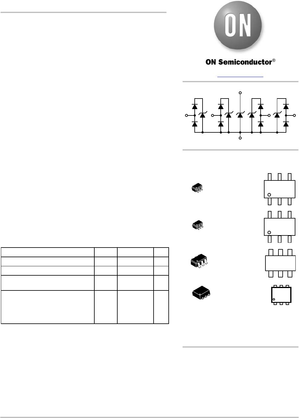
www.onsemi.com
MARKING
DIAGRAMS
X2 MG
G
XXX = Specific Device Code
M = Date Code
G = Pb−Free Package
1
6
1
SC−88
W1 SUFFIX
CASE 419B
(Note: Microdot may be in either location)
5
3
6
2
1
4
X4 MG
G
1
6
1
SC−88
W1 SUFFIX
CASE 419B
P4H
MG
G
1
6
TSOP−6
CASE 318G
STYLE 12
1
SOT−563
CASE 463A
P4MG
G
1
1
6
See detailed ordering and shipping information in the package
dimensions section on page 4 of this data sheet.
ORDERING INFORMATION
NUP4114 Series
www.onsemi.com
2
ELECTRICAL CHARACTERISTICS
(T
A
= 25°C unless otherwise noted)
Symbol
Parameter
I
PP
Maximum Reverse Peak Pulse Current
V
C
Clamping Voltage @ I
PP
V
RWM
Working Peak Reverse Voltage
I
R
Maximum Reverse Leakage Current @ V
RWM
V
BR
Breakdown Voltage @ I
T
I
T
Test Current
I
F
Forward Current
V
F
Forward Voltage @ I
F
P
pk
Peak Power Dissipation
C Capacitance @ V
R
= 0 and f = 1.0 MHz
*See Application Note AND8308/D for detailed explanations of
datasheet parameters.
Uni−Directional
I
PP
I
F
V
I
I
R
I
T
V
RWM
V
C
V
BR
V
F
ELECTRICAL CHARACTERISTICS (T
J
= 25°C unless otherwise specified)
Parameter
Symbol Conditions Min Typ Max Unit
Reverse Working Voltage V
RWM
5.5 V
Breakdown Voltage V
BR
I
T
= 1 mA, (Note 1) 5.5 6.5 V
Reverse Leakage Current I
R
V
RWM
= 5.5 V 1.0
mA
Clamping Voltage V
C
I
PP
= 1 A (Note 2) 8.3 10 V
I
PP
= 5 A (Note 3) 8.5 9.0 V
I
PP
= 8 A (Note 3) 9.2 10 V
ESD Clamping Voltage V
C
Per IEC61000−4−2 (Note 4) See Figures 1 & 2
Maximum Peak Pulse Current I
PP
8/20 ms Waveform (Note 3)
12 A
Junction Capacitance C
J
V
R
= 0 V, f = 1 MHz between I/O Pins and GND 0.6 pF
V
R
= 0 V, f = 1 MHz between I/O Pins 0.3 pF
1. V
BR
is measured at pulse test current I
T
.
2. Nonrepetitive current pulse (I/O to GND).
3. Nonrepetitive current pulse (Pin 5 to Pin 2)
4. For test procedure see Figures 3 and 4 and Application Note AND8307/D.
Figure 1. ESD Clamping Voltage Screenshot
Positive 8 kV Contact per IEC61000−4−2
Figure 2. ESD Clamping Voltage Screenshot
Negative 8 kV Contact per IEC61000−4−2
NUP4114 Series
www.onsemi.com
3
IEC 61000−4−2 Spec.
Level
Test Volt-
age (kV)
First Peak
Current
(A)
Current at
30 ns (A)
Current at
60 ns (A)
1 2 7.5 4 2
2 4 15 8 4
3 6 22.5 12 6
4 8 30 16 8
I
peak
90%
10%
IEC61000−4−2 Waveform
100%
I @ 30 ns
I @ 60 ns
t
P
= 0.7 ns to 1 ns
Figure 3. IEC61000−4−2 Spec
Figure 4. Diagram of ESD Test Setup
50 W
Cable
Device
Under
Test
Oscilloscope
ESD Gun
50 W
The following is taken from Application Note
AND8308/D − Interpretation of Datasheet Parameters
for ESD Devices.
ESD Voltage Clamping
For sensitive circuit elements it is important to limit the
voltage that an IC will be exposed to during an ESD event
to as low a voltage as possible. The ESD clamping voltage
is the voltage drop across the ESD protection diode during
an ESD event per the IEC61000−4−2 waveform. Since the
IEC61000−4−2 was written as a pass/fail spec for larger
systems such as cell phones or laptop computers it is not
clearly defined in the spec how to specify a clamping voltage
at the device level. ON Semiconductor has developed a way
to examine the entire voltage waveform across the ESD
protection diode over the time domain of an ESD pulse in the
form of an oscilloscope screenshot, which can be found on
the datasheets for all ESD protection diodes. For more
information on how ON Semiconductor creates these
screenshots and how to interpret them please refer to
AND8307/D.
Figure 5. 8/20 ms Pulse Waveform
100
90
80
70
60
50
40
30
20
10
0
020406080
t, TIME (ms)
% OF PEAK PULSE CURRENT
t
P
t
r
PULSE WIDTH (t
P
) IS DEFINED
AS THAT POINT WHERE THE
PEAK CURRENT DECAY = 8 ms
PEAK VALUE I
RSM
@ 8 ms
HALF VALUE I
RSM
/2 @ 20 ms

NUP4114HMR6T1G

Mfr. #:
Manufacturer:
ON Semiconductor
Description:
TVS Diodes / ESD Suppressors LOW CAP TVS ARRAY
Lifecycle:
New from this manufacturer.
Delivery:
DHL FedEx Ups TNT EMS
Payment:
T/T Paypal Visa MoneyGram Western Union