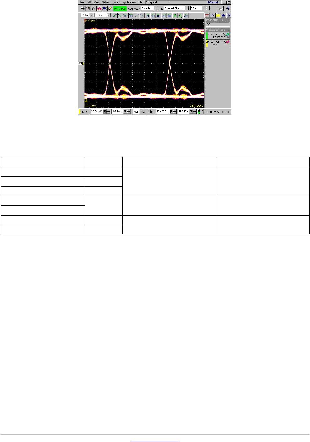
NUP4114HMR6T1G

NUP4114 Series
www.onsemi.com
4
Figure 6. 500 MHz Data Pattern
ORDERING INFORMATION
Device Marking Package Shipping
NUP4114UCLW1T2G X2
SC−88
(Pb−Free)
3000 / Tape & Reel
SZNUP4114UCLW1T2G X2
NUP4114UCW1T2G X4
NUP4114UPXV6T1G
P4
SOT−563
(Pb−Free)
4000 / Tape & Reel
NUP4114UPXV6T2G
NUP4114HMR6T1G P4H
TSOP−6
(Pb−Free)
3000 / Tape & Reel
SZNUP4114HMR6T1G P4H
For information on tape and reel specifications, including part orientation and tape sizes, please refer to our Tape and Reel Packaging
Specifications Brochure, BRD8011/D.
NUP4114 Series
www.onsemi.com
5
APPLICATIONS INFORMATION
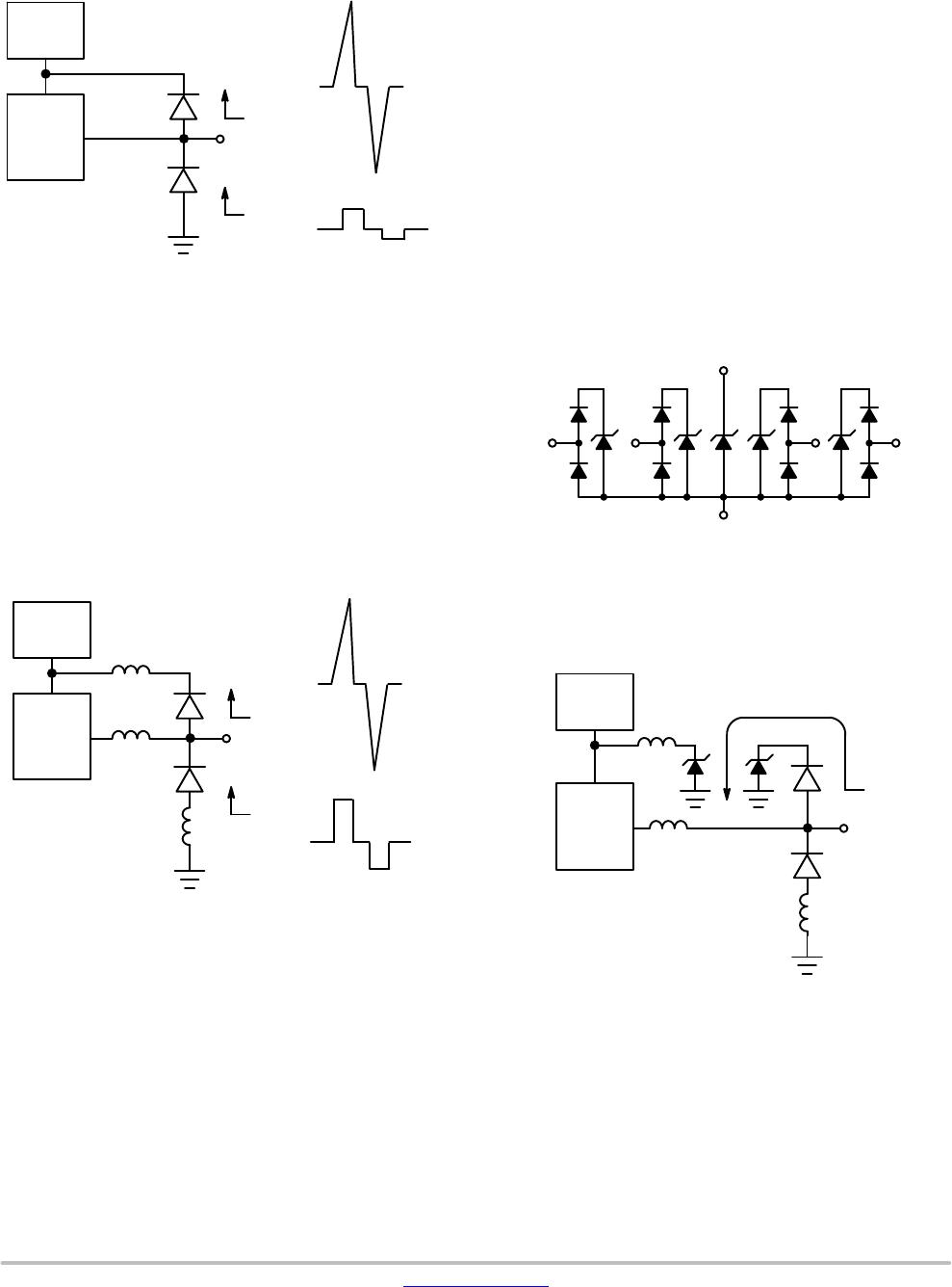
The new NUP4114 is a low capacitance ESD diode array
designed to protect sensitive electronics such as
communications systems, computers, and computer
peripherals against damage due to ESD events or transient
overvoltage conditions. Because of its low capacitance, it
can be used in high speed I/O data lines. The integrated
design of the NUP4114 offers low capacitance steering
diodes and an ESD diode integrated in a single package
(TSOP−6). If a transient condition occurs, the steering
diodes will drive the transient to the positive rail of the
power supply or to ground. This device protects the power
line against overvoltage conditions to avoid damage to the
power supply and any downstream components.
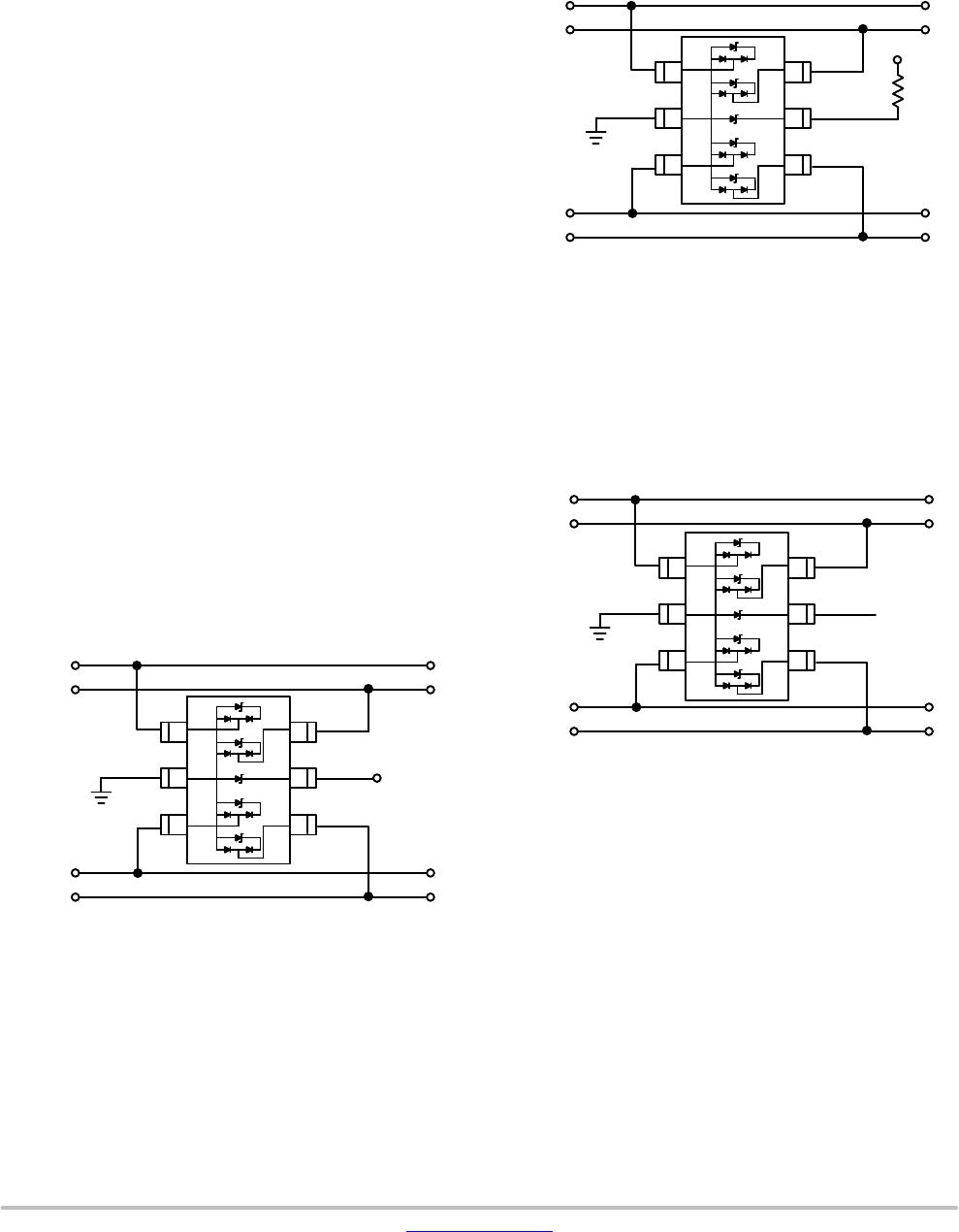
NUP4114 Configuration Options
The NUP4114 is able to protect up to four data lines
against transient overvoltage conditions by driving them to
a fixed reference point for clamping purposes. The steering
diodes will be forward biased whenever the voltage on the
protected line exceeds the reference voltage (V
f
or
V
CC
+ V
f
). The diodes will force the transient current to
bypass the sensitive circuit.
Data lines are connected at pins 1, 3, 4 and 6. The negative
reference is connected at pin 2. This pin must be connected
directly to ground by using a ground plane to minimize the
PCB’s ground inductance. It is very important to reduce the
PCB trace lengths as much as possible to minimize parasitic
inductances.
Option 1
Protection of four data lines and the power supply using
V
CC
as reference.
I/O 1
I/O 2
I/O 3
I/O 4
V
CC
6
5
4
1
2
3
For this configuration, connect pin 5 directly to the
positive supply rail (V
CC
), the data lines are referenced to
the supply voltage. The internal ESD diode prevents
overvoltage on the supply rail. Biasing of the steering diodes
reduces their capacitance.
Option 2
Protection of four data lines with bias and power supply
isolation resistor.
V
CC
10 k
I/O 1
I/O 2
I/O 3
I/O 4
6
5
4
1
2
3
The NUP4114 can be isolated from the power supply by
connecting a series resistor between pin 5 and V
CC
. A 10 kW
resistor is recommended for this application. This will
maintain a bias on the internal ESD and steering diodes,
reducing their capacitance.
Option 3
Protection of four data lines using the internal ESD diode
as reference.
I/O 1
I/O 2
I/O 3
I/O 4
NC
6
5
4
1
2
3
In applications lacking a positive supply reference or
those cases in which a fully isolated power supply is
required, the internal ESD can be used as the reference. For
these applications, pin 5 is not connected. In this
configuration, the steering diodes will conduct whenever the
voltage on the protected line exceeds the working voltage of
the ESD plus one diode drop (V
C
= V
f
+ VESD).
ESD Protection of Power Supply Lines
When using diodes for data line protection, referencing to
a supply rail provides advantages. Biasing the diodes
reduces their capacitance and minimizes signal distortion.
NUP4114 Series
www.onsemi.com
6
Implementing this topology with discrete devices does have
disadvantages. This configuration is shown below:
V
CC
D1
D2
Data Line
I
ESDpos
I
ESDneg
VF + V
CC
−VF
I
ESDpos
I
ESDneg
Power
Supply
Protected
Device
Looking at the figure above, it can be seen that when a
positive ESD condition occurs, diode D1 will be forward
biased while diode D2 will be forward biased when a
negative ESD condition occurs. For slower transient
conditions, this system may be approximated as follows:
For positive pulse conditions:
V
c
= V
CC
+ V
fD1
For negative pulse conditions:
V
c
= −V
fD2
ESD events can have rise times on the order of some
number of nanoseconds. Under these conditions, the effect
of parasitic inductance must be considered. A pictorial
representation of this is shown below.
V
CC
D1
D2
Data Line
I
ESDpos
I
ESDneg
V
C
= V
CC
+ Vf + (L diESD/d
t)
I
ESDpos
I
ESDneg
Power
Supply
Protected
Device
V
C
= −Vf − (L diESD/dt
)
An approximation of the clamping voltage for these fast
transients would be:
For positive pulse conditions:
V
c
= V
CC
+ Vf + (L diESD/dt)
For negative pulse conditions:
V
c
= −V
f
– (L diESD/dt)
As shown in the formulas, the clamping voltage (V
c
) not
only depends on the Vf of the steering diodes but also on the
L di
ESD/dt factor. A relatively small trace inductance can
result in hundreds of volts appearing on the supply rail. This
endangers both the power supply and anything attached to
that rail. This highlights the importance of good board
layout. Taking care to minimize the effects of parasitic
inductance will provide significant benefits in transient
immunity.
Even with good board layout, some disadvantages are still
present when discrete diodes are used to suppress ESD
events across datalines and the supply rail. Discrete diodes
with good transient power capability will have larger die and
therefore higher capacitance. This capacitance becomes
problematic as transmission frequencies increase. Reducing
capacitance generally requires reducing die size. These
small die will have higher forward voltage characteristics at
typical ESD transient current levels. This voltage combined
with the smaller die can result in device failure.
The ON Semiconductor NUP4114 was developed to
overcome the disadvantages encountered when using
discrete diodes for ESD protection. This device integrates an
ESD diode within a network of steering diodes.
Figure 7. NUP4114 Equivalent Circuit
5
3
6
2
1
4
During an ESD condition, the ESD current will be driven
to ground through the ESD diode as shown below.
V
CC
D1
D2
Data Line
I
ESDpos
Power
Supply
Protected
Device
The resulting clamping voltage on the protected IC will
be:
V
c
= VF + V
ESD
.
The clamping voltage of the ESD diode depends on the
magnitude of the ESD current. The steering diodes are fast
switching devices with unique forward voltage and low
capacitance characteristics.

NUP4114HMR6T1G

Mfr. #:
Manufacturer:
ON Semiconductor
Description:
TVS Diodes / ESD Suppressors LOW CAP TVS ARRAY
Lifecycle:
New from this manufacturer.
Delivery:
DHL FedEx Ups TNT EMS
Payment:
T/T Paypal Visa MoneyGram Western Union