6.4210
IDT71V67703, IDT71V67903, 256K x 36, 512K x 18, 3.3V Synchronous SRAMS with
3.3V I/O, Flow-Through Outputs, Single Cycle Deselect Commercial and Industrial Temperature Ranges
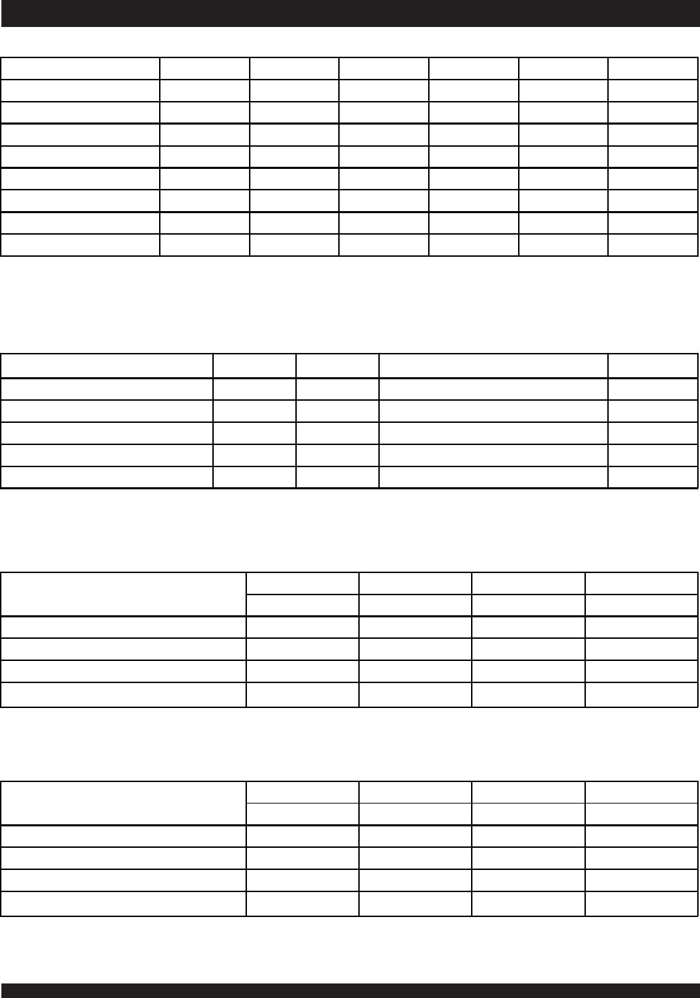
Synchronous Truth Table
(1,3)
NOTES:
1. L = VIL, H = VIH, X = Don’t Care.
2. OE is an asynchronous input.
3. ZZ - low for the table.
Operation Address
Used
CE
CS
0
CS
1
ADSP ADSC ADV GW BWE BWx OE
(2 )
CLK I/O
Deselected Cycle, Power Down None H X X X L X X X X X HI-Z
Deselected Cycle, Power Down None L X H L X X X X X X HI-Z
Deselected Cycle, Power Down None L L X L X X X X X X HI-Z
Deselected Cycle, Power Down None L X H X L X X X X X HI-Z
Deselected Cycle, Power Down None L L X X L X X X X X HI-Z
Read Cycle, Begin Burst External L H L L X X X X X L D
OUT
Read Cycle, Begin Burst External L H L L X X X X X H
HI-Z
Read Cycle, Begin Burst External L H L H L X H H X L D
OUT
Read Cycle, Begin Burst External L H L H L X H L H L D
OUT
Read Cycle, Begin Burst External L H L H L X H L H H HI-Z
Write Cycle, Begin Burst External L H L H L X H L L X D
IN
Write Cycle, Begin Burst External L H L H L X L X X X D
IN
Read Cycle, Continue Burst Next X X X H H L H H X L D
OUT
Read Cycle, Continue Burst Next X X X H H L H H X H HI-Z
Read Cycle, Continue Burst Next X X X H H L H X H L D
OUT
Read Cycle, Continue Burst Next X X X H H L H X H H HI-Z
Read Cycle, Continue Burst Next H X X X H L H H X L D
OUT
Read Cycle, Continue Burst Next H X X X H L H H X H HI-Z
Read Cycle, Continue Burst Next H X X X H L H X H L
D
OUT
Read Cycle, Continue Burst Next H X X X H L H X H H HI-Z
Write Cycle, Continue Burst Next X X X H H L H L L X D
IN
Write Cycle, Continue Burst Next X X X H H L L X X X D
IN
Write Cycle, Continue Burst Next H X X X H L H L L X D
IN
Write Cycle, Continue Burst Next H X X X H L L X X X D
IN
Read Cycle, Suspend Burst Current X X X H H H H H X L
D
OUT
Read Cycle, Suspend Burst Current X X X H H H H H X H HI-Z
Read Cycle, Suspend Burst Current X X X H H H H X H L D
OUT
Read Cycle, Suspend Burst Current X X X H H H H X H H HI-Z
Read Cycle, Suspend Burst Current H X X X H H H H X L D
OUT
Read Cycle, Suspend Burst Current H X X X H H H H X H HI-Z
Read Cycle, Suspend Burst Current H X X X H H H X H L
D
OUT
Read Cycle, Suspend Burst Current H X X X H H H X H H HI-Z
Write Cycle, Suspend Burst Current X X X H H H H L L X D
IN
Write Cycle, Suspend Burst Current X X X H H H L X X X D
IN
Write Cycle, Suspend Burst Current H X X X H H H L L X D
IN
Write Cycle, Suspend Burst Current H X X X H H L X X X D
IN
5309 tbl 11
6.42
11
IDT71V67703, IDT71V67903, 256K x 36, 512K x 18, 3.3V Synchronous SRAMS with
3.3V I/O, Flow-Through Outputs, Single Cycle Deselect Commercial and Industrial Temperature Ranges
Linear Burst Sequence Table ( LBO=VSS)
Synchronous Write Function Truth Table
(1, 2)
Asynchronous Truth Table
(1)
Interleaved Burst Sequence Table ( LBO=VDD)
NOTES:
1. L = V
IL, H = VIH, X = Don’t Care.
2. BW
3 and BW4 are not applicable for the IDT71V67903.
3. Multiple bytes may be selected during the same cycle.
NOTES:
1. L = VIL, H = VIH, X = Don’t Care.
2. Synchronous function pins must be biased appropriately to satisfy operation requirements.
NOTE:
1. Upon completion of the Burst sequence the counter wraps around to its initial state.
NOTE:
1. Upon completion of the Burst sequence the counter wraps around to its initial state.
Operation
GW BWE BW
1
BW
2
BW
3
BW
4
Read HHXXXX
Read HLHHHH
Write all Bytes LXXXXX
Write all Bytes HLLLLL
Write Byte 1
(3 )
HLLHHH
Write Byte 2
(3 )
HLHLHH
Write Byte 3
(3 )
HLHHLH
Write Byte 4
(3 )
HLHHHL
5309 tbl 12
Operation
(2)
OE
ZZ I/O Status Power
Read L L Data Out Active
Read H L High-Z Active
Write X L High-Z – Data In Active
Deselected X L High-Z Standby
Sleep Mode X H High-Z Sleep
5309 tbl 13
Sequence 1 Sequence 2 Sequence 3 Sequence 4
A1 A0 A1 A0 A1 A0 A1 A0
First Address 00011011
Second Address 0 1 0 0 1 1 1 0
Third Address 1 0 1 1 0 0 0 1
Fourth Address
(1)
11100100
5309 tbl 14
Sequence 1 Sequence 2 Sequence 3 Sequence 4
A1 A0 A1 A0 A1 A0 A1 A0
First Address 00011011
Second Address 0 1 1 0 1 1 0 0
Third Address 1 0 1 1 0 0 0 1
Fourth Address
(1)
11000110
5309 tbl 15
6.4212
IDT71V67703, IDT71V67903, 256K x 36, 512K x 18, 3.3V Synchronous SRAMS with
3.3V I/O, Flow-Through Outputs, Single Cycle Deselect Commercial and Industrial Temperature Ranges
AC Electrical Characteristics
(VDD = 3.3V ±5%, Commercial and Industrial Temperature Ranges)
7.5ns 8ns 8.5ns
Symbol Parameter Min.Max.Min.Max.Min.Max.Unit
Clock Parameter
t
CY C
Clock Cycle Time 8.5
____
10
____
11. 5
____
ns
t
CH
(1)
Clock High Pulse Width 3
____
4
____
4.5
____
ns
t
CL
(1 )
Clock Low Pulse Width 3
____
4
____
4.5
____
ns
Output Parameters
t
CD
Clock High to Valid Data
____
7.5
____
8
____
8.5 ns
t
CD C
Clock High to Data Change 2
____
2
____
2
____
ns
t
CL Z
(2)
Clock High to Output Active 0
____
0
____
0
____
ns
t
CHZ
(2 )
Clock High to Data High-Z 2 3.5 2 3.5 2 3.5 ns
t
OE
Output Enable Access Time
____
3.5
____
3.5
____
3.5 ns
t
OL Z
(2)
Output Enable Low to Output Active 0
____
0
____
0
____
ns
t
OHZ
(2 )
Output Enable High to Output High-Z
____
3.5
____
3.5
____
3.5 ns
Set Up Times
t
SA
Address Setup Time 1.5
____
2
____
2
____
ns
t
SS
Address Status Setup Time 1.5
____
2
____
2
____
ns
t
SD
Data In Setup Time 1.5
____
2
____
2
____
ns
t
SW
Write Setup Time 1.5
____
2
____
2
____
ns
t
SAV
Address Advance Setup Time 1.5
____
2
____
2
____
ns
t
SC
Chip Enable/Select Setup Time 1.5
____
2
____
2
____
ns
Hold Times
t
HA
Address Hold Time 0.5
____
0.5
____
0.5
____
ns
t
HS
Address Status Hold Time 0.5
____
0.5
____
0.5
____
ns
t
HD
Data In Hold Time 0.5
____
0.5
____
0.5
____
ns
t
HW
Write Hold Time 0.5
____
0.5
____
0.5
____
ns
t
HAV
Address Advance Hold Time 0.5
____
0.5
____
0.5
____
ns
t
HC
Chip Enable/Select Hold Time 0.5
____
0.5
____
0.5
____
ns
Sleep Mode and Configuration Parameters
t
ZZP W
ZZ Pulse Width 100
____
100
____
100
____
ns
t
ZZR
(3)
ZZ Recovery Time 100
____
100
____
100
____
ns
t
CF G
(4)
Configuration Set-up Time 34
____
40
____
50
____
ns
5309 tbl 16
NOTES:
1. Measured as HIGH above VIH and LOW below VIL.
2. Transition is measured ±200mV from steady-state.
3. Device must be deselected when powered-up from sleep mode.
4. tCFG is the minimum time required to configure the device based on the LBO input. LBO is a static input and must not change during normal operation.

71V67703S75BQGI

Mfr. #:
Manufacturer:
IDT
Description:
SRAM 9M 3.3V PBSRAM SLOW F/T
Lifecycle:
New from this manufacturer.
Delivery:
DHL FedEx Ups TNT EMS
Payment:
T/T Paypal Visa MoneyGram Western Union