IXYS Reserves the Right to Change Limits, Test Conditions, and Dimensions.
IXXH50N60C3D1
IXYS MOSFETs and IGBTs are covered 4,835,592 4,931,844 5,049,961 5,237,481 6,162,665 6,404,065 B1 6,683,344 6,727,585 7,005,734 B2 7,157,338B2
by one or more of the following U.S. patents: 4,860,072 5,017,508 5,063,307 5,381,025 6,259,123 B1 6,534,343 6,710,405 B2 6,759,692 7,063,975 B2
4,881,106 5,034,796 5,187,117 5,486,715 6,306,728 B1 6,583,505 6,710,463 6,771,478 B2 7,071,537
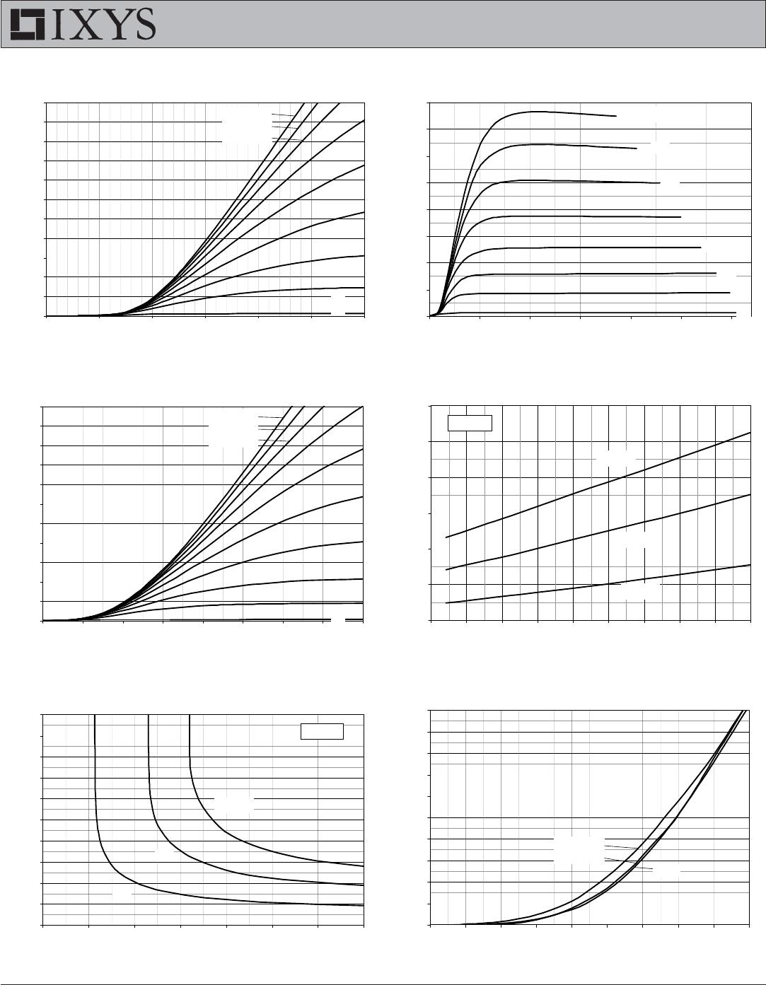
Symbol Test Conditions Characteristic Values
(T
J
= 25°C Unless Otherwise Specified) Min. Typ. Max.
g
fs
I
C
= 36A, V
CE
= 10V, Note 1 11 18 S
C
ie
s
2320 pF
C
oes
V
CE
= 25V, V
GE
= 0V, f = 1MHz 138 pF
C
res
42 pF
Q
g
64 nC
Q
ge
I
C
= 36A, V
GE
= 15V, V
CE
= 0.5 • V
CES
18 nC
Q
gc
25 nC
t
d(on)
24 ns
t
ri
40 ns
E
on
0.72 mJ
t
d(off)
62 100 ns
t
fi
42 ns
E
of
f
0.33 0.55 mJ
t
d(on)
25 ns
t
ri
44 ns
E
on
1.46 mJ
t
d(off)
80 ns
t
fi
90 ns
E
off
0.48 mJ
R
thJC
0.25 °C/W
R
thCS
0.21 °C/W
Inductive load, T
J
= 25°C
I
C
= 36A, V
GE
= 15V
V
CE
= 360V, R
G
= 5Ω
Note 2
Notes:
1. Pulse test, t ≤ 300μs, duty cycle, d ≤ 2%.
2. Switching times & energy losses may increase for higher V
CE
(clamp), T
J
or R
G
.
e
∅ P
TO-247 (IXXH) Outline
1 2 3
Terminals: 1 - Gate 2 - Collector
3 - Emitted
Dim. Millimeter Inches
Min. Max. Min. Max.
A 4.7 5.3 .185 .209
A
1
2.2 2.54 .087 .102
A
2
2.2 2.6 .059 .098
b 1.0 1.4 .040 .055
b
1
1.65 2.13 .065 .084
b
2
2.87 3.12 .113 .123
C .4 .8 .016 .031
D 20.80 21.46 .819 .845
E 15.75 16.26 .610 .640
e 5.20 5.72 0.205 0.225
L 19.81 20.32 .780 .800
L1 4.50 .177
∅P 3.55 3.65 .140 .144
Q 5.89 6.40 0.232 0.252
R 4.32 5.49 .170 .216
S 6.15 BSC 242 BSC
Inductive load, T
J
= 150°C
I
C
= 36A, V
GE
= 15V
V
CE
= 360V, R
G
= 5Ω
Note 2
Reverse Diode (FRED)
Symbol Test Conditions Characteristic Values
(T
J
= 25°C Unless Otherwise Specified) Min. Typ. Max.
V
F
I
F
= 30A, V
GE
= 0V, Note 1 2.7 V
T
J
= 150°C 1.6 V
I
RM
T
J
= 100°C 4 A
t
rr
T
J
= 100°C 100 ns
25 ns
R
thJC
0.9 °C/W
I
F
= 30A, V
GE
= 0V, -di
F
/dt = 100A/μs,
V
R
= 100V
I
F
= 1A, V
GE
= 0V, -di
F
/dt = 100A/μs, V
R
= 30V
PRELIMINARY TECHNICAL INFORMATION
The product presented herein is under development. The Technical Specifications offered are derived
from data gathered during objective characterizations of preliminary engineering lots; but also may yet
contain some information supplied during a pre-production design evaluation. IXYS reserves the right
to change limits, test conditions, and dimensions without notice.