Expand menu
Hello, Sign in
My Account
0
Cart
Home
Products
Sensors
Semiconductors
Passive Components
Connectors
Power
Electromechanical
Optoelectronics
Circuit Protection
Integrated Circuits - ICs
Main Products
Manufacturers
Blog
Services
About OMO
About Us
Contact Us
Check Stock
IXXH50N60C3D1
P1-P3
P4-P6
P7-P7
IXYS Reserves the Right to Change Limits, Test Conditions, and Dimensions.
IXXH50N60C3D1
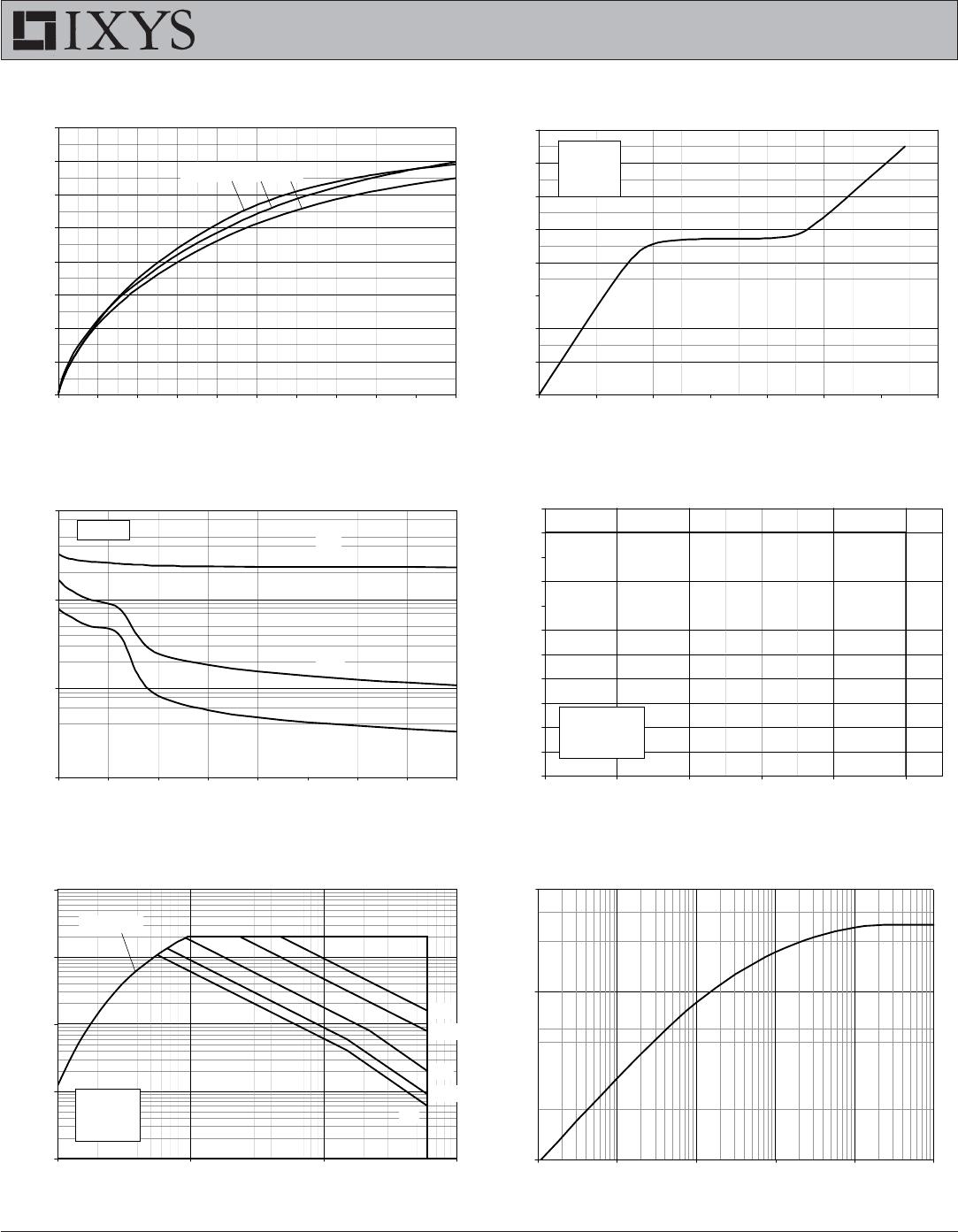
Fig. 11
. M
ax
im
um
T
rans
ient Therm
al Impedanc
e
0.01
0.1
1
0.00001
0.0001
0.001
0.01
0.1
1
Puls
e
W
idth -
S
e
c
ond
Z
(th)JC
- ºC
/ W
Fig. 1
2. M
ax
im
um
T
ransie
nt Ther
m
al Im
pedanc
e
aa sss
0.4
Fig. 7. Transc
onducta
nce
0
4
8
12
16
20
24
28
32
0
1
02
03
04
05
06
0
7
08
09
0
1
0
0
I
C
- Am
peres
g
f s
-
Si
emens
T
J
= - 40ºC, 25ºC, 150ºC
Fi
g.
10. Rever
se-Bias Safe Op
eratin
g Area
0
10
20
30
40
50
60
70
80
90
100
110
100
200
300
400
500
600
V
CE
- Vo
l
ts
I
C
- Amperes
T
J
= 150ºC
R
G
= 5
Ω
dv
/
dt <
10V / n
s
Fig. 8. G
ate
Charge
0
2
4
6
8
10
12
14
16
0
1
02
0
3
04
0
5
06
07
0
Q
G
- Nan
oCou
l
om
b
s
V
GE
- Vol
ts
V
CE
= 300V
I
C
= 36
A
I
G
= 10
mA
Fig. 9. Ca
pac
itanc
e
10
100
1,000
10,000
0
5
10
15
20
25
30
35
40
V
CE
- Vol
ts
Capacit
ance - Pi
coFarads
f
= 1 MH
z
C
ies
C
oes
C
res
Fi
g.
11. Fo
rward
-Bi
as Safe Operati
ng Area
0.1
1
10
100
1000
1
10
100
1000
V
DS
- Vo
l
ts
I
D
- Amperes
T
J
= 175ºC
T
C
= 25ºC
Single Pulse
25µs
1ms
10ms
V
CE(sat)
Lim
it
DC
100µs
© 2013 IXYS CORPORATION, All Rights Reserved
IXXH50N60C3D1
Fig. 13
. Inductive
Swit
ching Ene
r
gy
L
os
s vs.
Gate Resistance
0.2
0.4
0.6
0.8
1.0
1.2
5
1
01
52
02
53
03
54
04
55
0
R
G
- Oh
m
s
E
off
- M
illiJ
o
ule
s
0.5
1.0
1.5
2.0
2.5
3.0
3.5
4.0
4.5
5.0
5.5
E
on
- M
illiJ
o
ule
s
E
off
E
on
- - - -
T
J
= 150ºC , V
GE
= 15
V
V
CE
= 36
0V
I
C
= 36A
I
C
= 54A
Fig. 16
. Inductiv
e T
urn-of
f Sw
itching Tim
es v
s.
Gate Resistance
50
60
70
80
90
100
110
120
5
1
01
52
02
53
03
54
04
55
0
R
G
- Oh
m
s
t
f i
- Nanoseconds
0
50
100
150
200
250
300
350
t
d
(
off
)
- Nanoseconds
t
f i
t
d(off)
- - - -
T
J
= 150ºC,
V
GE
= 15V
V
CE
= 36
0V
I
C
= 36A
I
C
= 54A
Fig
. 14. In
ducti
ve Switching
Energy L
oss vs.
Collec
tor Curr
ent
0.1
0.2
0.3
0.4
0.5
0.6
0.7
18
22
26
30
34
38
42
46
50
54
I
C
- A
m
p
eres
E
off
- M
illiJ
o
ule
s
0.0
0.5
1.0
1.5
2.0
2.5
3.0
E
on
- M
illiJ
ou
le
s
E
off
E
on
- - - -
R
G
= 5
Ω
,
V
GE
= 15V
V
CE
= 36
0V
T
J
= 150ºC
T
J
= 25
ºC
Fig. 15
. Inductive
Swit
ching Ene
r
gy
Lo
s
s vs.
Junc
tion T
em
perat
ure
0.1
0.2
0.3
0.4
0.5
0.6
0.7
0.8
0.9
25
50
75
100
125
150
T
J
- Deg
rees Cen
tig
rad
e
E
off
- M
illiJ
ou
les
0.2
0.6
1.0
1.4
1.8
2.2
2.6
3.0
3.4
E
on
- M
illiJ
ou
les
E
of
f
E
on
- - - -
R
G
= 5
Ω
,
V
GE
= 15V
V
CE
= 3
60
V
I
C
= 36
A
I
C
= 54A
Fig. 1
7. Induct
ive
T
urn-off
Swit
ching Tim
es
vs
.
Collec
tor Current
0
20
40
60
80
100
120
140
160
18
22
26
30
34
38
42
46
50
54
I
C
- A
m
p
eres
t
f i
- Nanoseconds
40
50
60
70
80
90
100
110
120
t
d(off)
- Nanoseconds
t
f i
t
d(off)
- - - -
R
G
= 5
Ω
, V
GE
= 15V
V
CE
= 3
60
V
T
J
=
150ºC
T
J
= 25º
C
Fig. 18
. Inductiv
e T
urn-
o
f
f Sw
itc
hing T
im
es v
s.
Juncti
on T
em
p
erature
20
30
40
50
60
70
80
90
100
110
120
25
50
75
100
125
150
T
J
- Deg
rees Cen
tig
rad
e
t
f i
- Nanoseconds
40
45
50
55
60
65
70
75
80
85
90
t
d
(
off
)
- Nanoseconds
t
f i
t
d(off)
- - - -
R
G
= 5
Ω
, V
GE
= 15V
V
CE
= 36
0V
I
C
= 54A
I
C
= 36A
IXYS Reserves the Right to Change Limits, Test Conditions, and Dimensions.
IXXH50N60C3D1
Fig. 20
.
Induct
ive Turn-on Swit
ching T
im
es v
s.
Co
ll
ecto
r C
ur
ren
t
0
10
20
30
40
50
60
70
80
90
18
22
26
30
34
38
42
46
5
0
54
I
C
- Am
p
eres
t
r i
- Nanos
econds
21
22
23
24
25
26
27
28
29
30
t
d
(
on
)
- Nanoseconds
t
r i
t
d(on)
- - - -
R
G
= 5
Ω
, V
GE
= 15V
V
CE
= 360V
T
J
= 150
ºC
T
J
= 25º
C
Fig. 21
. Inductive
T
urn-on Sw
itching Ti
m
es
vs.
Junct
ion T
em
pera
ture
10
30
50
70
90
110
130
25
50
75
100
1
25
150
T
J
-
D
e
gre
e
s
C
e
ntigr
a
de
t
r i
- Nan
osecon
ds
20
22
24
26
28
30
32
t
d
(
on
)
- Na
nosec
onds
t
r i
t
d(on)
- - - -
R
G
= 5
Ω
, V
GE
= 15V
V
CE
= 360V
I
C
= 54
A
I
C
= 36
A
Fig. 19
.
Induct
ive Tu
rn-on S
witc
hing T
im
es v
s.
Gate Resi
stan
ce
30
40
50
60
70
80
90
100
110
120
130
140
5
1
01
52
02
5
3
03
54
04
5
5
0
R
G
- Oh
m
s
t
r i
- Nanoseconds
0
10
20
30
40
50
60
70
80
90
100
110
t
d
(
on
)
- Nan
oseco
nd
s
t
r i
t
d(on)
- - - -
T
J
= 150ºC, V
GE
= 15
V
V
CE
=
360V
I
C
= 54A
I
C
= 36A
P1-P3
P4-P6
P7-P7
IXXH50N60C3D1
Mfr. #:
Buy IXXH50N60C3D1
Manufacturer:
Description:
IGBT Transistors XPT IGBT C3-Class 600V/100Amp CoPacked
Lifecycle:
New from this manufacturer.
Delivery:
DHL
FedEx
Ups
TNT
EMS
Payment:
T/T
Paypal
Visa
MoneyGram
Western
Union
Products related to this Datasheet
IXXH50N60C3D1