6.4220
IDT71V65603, IDT71V65803, 256K x 36, 512K x 18, 3.3V Synchronous SRAMs with
ZBT
™™
™™
™ Feature, 3.3V I/O, Burst Counter, and Pipelined Outputs Commercial and Industrial Temperature Ranges
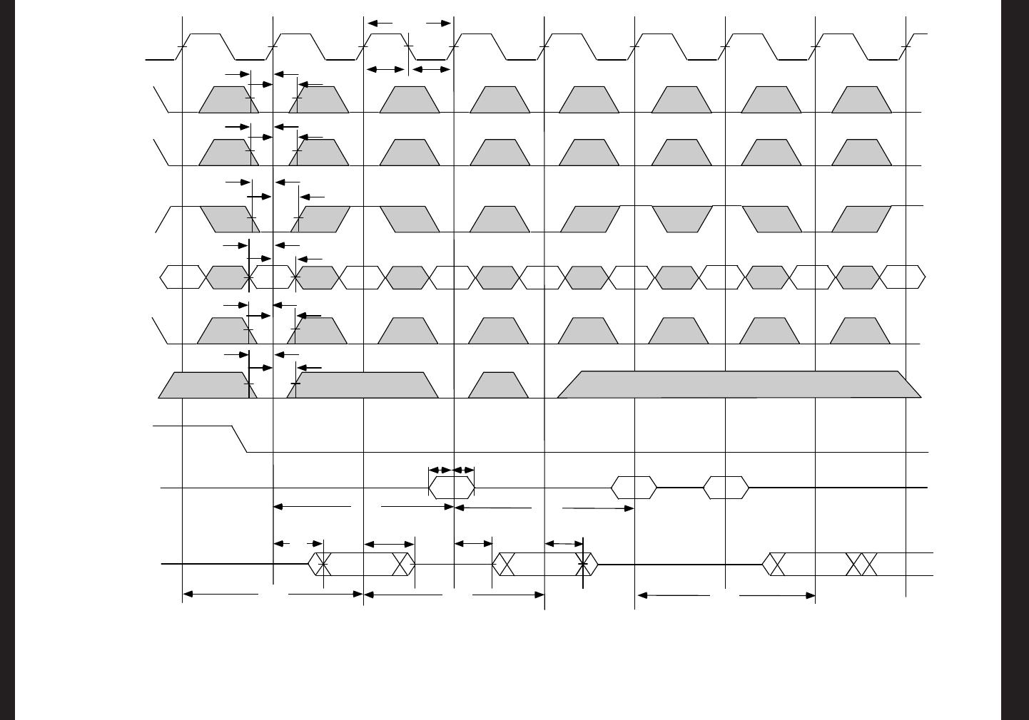
NOTES:
1. Q (A
1) represents the first output from the external address A1. D (A2) represents the input data to the SRAM corresponding to address A2.
2. CE
2 timing transitions are identical but inverted to the CE1 and CE2 signals. For example, when CE1 and CE2 are LOW on this waveform, CE2 is HIGH.
3. CEN when sampled high on the rising edge of clock will block that L-H transition of the clock from propogating into the SRAM. The part will behave as if the L-H clock transition did not
occur. All internal registers in the SRAM will retain their previous state.
4. Individual Byte Write signals (BWx) must be valid on all write and burst-write cycles. A write cycle is initiated when R/W signal is sampled LOW. The byte write information comes in two
cycles before the actual data is presented to the SRAM.
Timing Waveform of CEN Operation
(1,2,3,4)
t
H
E
t
S
E
R
/
W
A
1
A
2
C
L
K
C
E
N
A
D
V
/
L
D
A
D
D
R
E
S
S
B
W
1
-
B
W
4
O
E
D
A
T
A
O
U
T
Q
(
A
3
)
t
C
D
t
C
L
Z
t
C
H
Z
t
C
H
t
C
L
t
C
Y
C
t
H
C
t
S
C
D
(
A
2
)
t
S
D
t
H
D
t
C
D
C
A
4
A
5
t
H
A
D
V
t
S
A
D
V
t
H
W
t
S
W
t
H
A
t
S
A
A
3
t
H
B
t
S
B
D
A
T
A
I
N
Q
(
A
1
)
5
3
0
4
d
r
w
0
9
Q
(
A
1
)
B
(
A
2
)
C
E
1
,
C
E
2
(
2
)