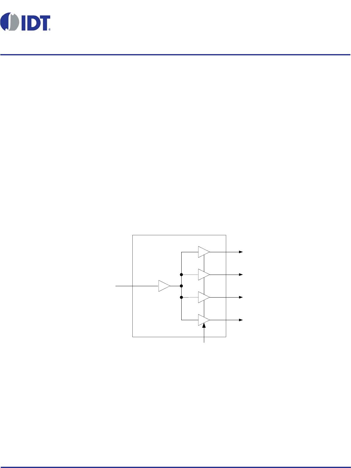
LOW SKEW 1 TO 4 CLOCK BUFFER 2 REVISION A 03/18/15
553S DATASHEET
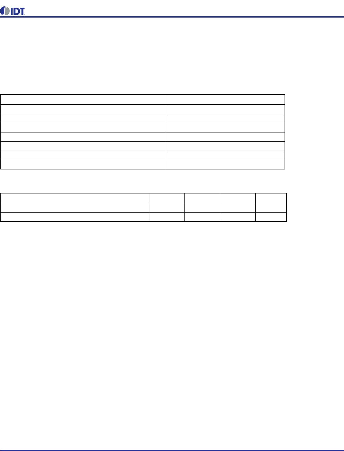
Pin Assignments
Pin Descriptions
External Components
A minimum number of external components are required for proper operation. A decoupling capacitor of 0.01 µF should be
connected between VDD on pin 1 and GND on pin 4, as close to the device as possible. A 33 series terminating resistor may
be used on each clock output if the trace is longer than 1 inch.
To achieve the low output skew that the 553S is capable of, careful attention must be paid to board layout. Essentially, all four
outputs must have identical terminations, identical loads and identical trace geometries. If they do not, the output skew will be
degraded. For example, using a 30 series termination on one output (with 33 on the others) will cause at least 15 ps of skew.
Pin
Number
Pin
Name
Pin
Type
Pin Description
1 VDD Power Connect to +1.8V, +2.5 V, or +3.3 V.
2 Q0 Output Clock output 0.
3 Q1 Output Clock output 1.
4 GND Power Connect to ground.
5 ICLK Input Clock input.
6 Q2 Output Clock Output 2.
7 Q3 Output Clock Output 3.
8 OE Input Output Enable. Tri-states outputs when low. Connect to VDD for normal operation.
1
2
3
VDD
4
Q0
Q1
Q3
GND
Q2
ICLK
8
7
6
5
OE
8-pin SOIC
1
2
3
VDD
4
Q0
Q1
Q3
GND
Q2
ICLK
8
7
6
5
OE
8-pin DFN