REVISION A 03/18/15 5 LOW SKEW 1 TO 4 CLOCK BUFFER
553S DATASHEET
AC Electrical Characteristics
(VDD = 1.8V, 2.5V, 3.3V)
VDD = 1.8V ±5%, Ambient Temperature -40° to +105°C, unless stated otherwise
VDD = 2.5 V ±5%, Ambient Temperature -40° to +105°C, unless stated otherwise
VDD = 3.3 V ±5%, Ambient Temperature -40° to +105°C, unless stated otherwise
Notes:
1. With rail to rail input clock
2. Between any 2 outputs with equal loading.
3. Duty cycle on outputs will match incoming clock duty cycle. Consult IDT for tight duty cycle clock generators.
Parameter Symbol Conditions Min. Typ. Max. Units
Input Frequency 0 200 MHz
Output Rise Time t
OR
0.36 to 1.44 V, C
L
=5 pF 0.6 1.0 ns
Output Fall Time t
OF
1.44 to 0.36 V, C
L
=5 pF 0.6 1.0 ns
Propagation Delay Note 1 2.5 3 3.5 ns
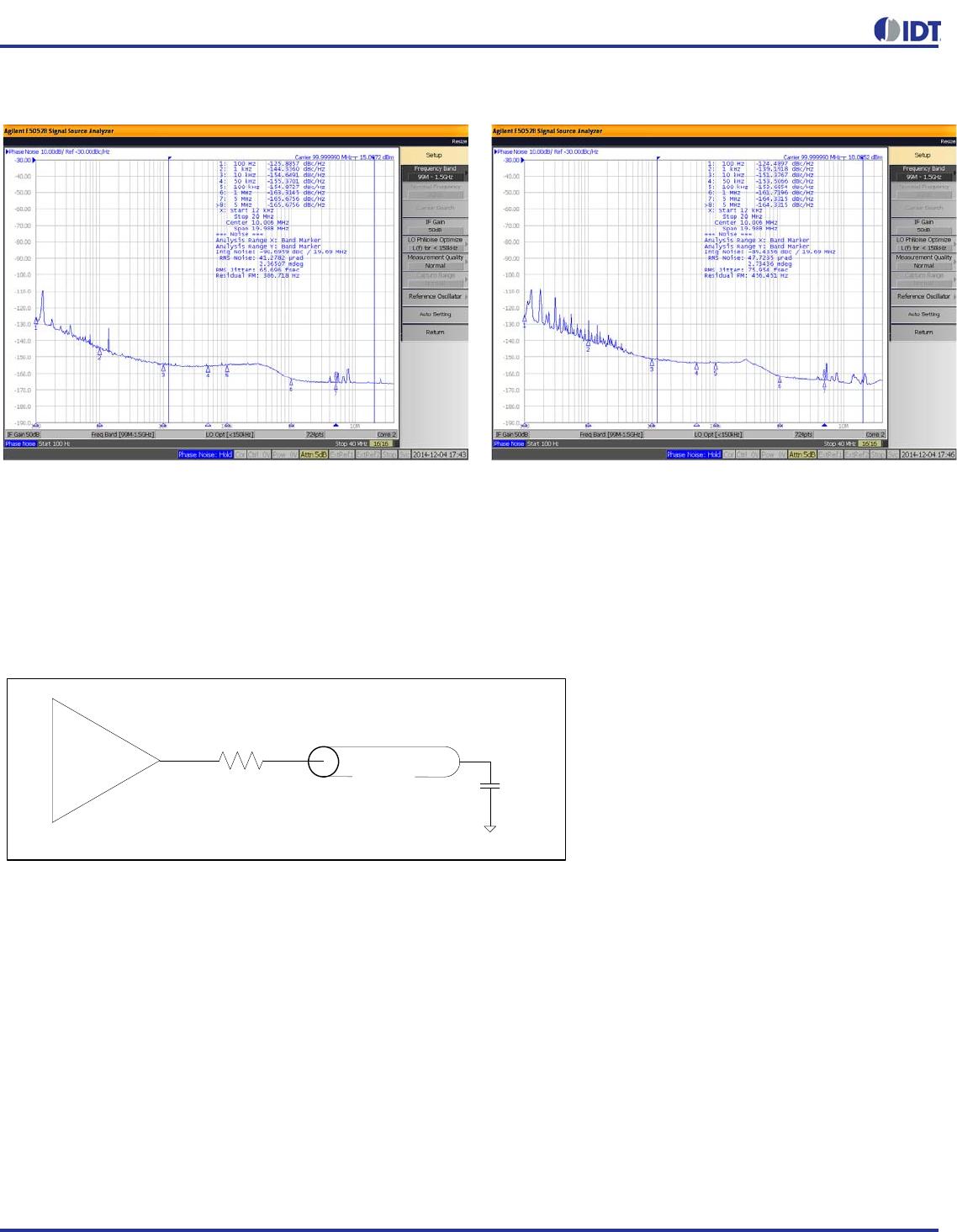
Buffer Additive Phase Jitter, RMS 125MHz, Integration Range: 12kHz-20MHz 0.05 ps
Output to Output Skew Note 2 Rising edges at VDD/2 50 65 ps
Device to Device Skew Rising edges at VDD/2 200 ps
Start-up Time t
START-UP
Part start-up time for valid outputs after
VDD ramp-up
2ms
Output Enable Time t
EN
C
L
< 5 pF 3 cycles
Output Disable Time t
DIS
C
L
< 5 pF 3 cycles
Parameter Symbol Conditions Min. Typ. Max. Units
Input Frequency 0 200 MHz
Output Rise Time t
OR
0.5 to 2.0 V, C
L
=5 pF 0.6 1.0 ns
Output Fall Time t
OF
2.0 to 0.5 V, C
L
=5 pF 0.6 1.0 ns
Propagation Delay Note 1 3 3.5 4 ns
Buffer Additive Phase Jitter, RMS 125MHz, Integration Range: 12kHz-20MHz 0.05 ps
Output to Output Skew Note 2 Rising edges at VDD/2 40 65 ps
Device to Device Skew Rising edges at VDD/2 200 ps
Start-up Time t
START-UP
Part start-up time for valid outputs after
VDD ramp-up
2ms
Output Enable Time t
EN
C
L
< 5 pF 3 cycles
Output Disable Time t
DIS
C
L
< 5 pF 3 cycles
Parameter Symbol Conditions Min. Typ. Max. Units
Input Frequency 0 200 MHz
Output Rise Time t
OR
0.66 to 2.64 V, C
L
=5 pF 0.6 1.0 ns
Output Fall Time t
OF
2.64 to 0.66 V, C
L
=5 pF 0.6 1.0 ns
Propagation Delay Note 1 2.5 3 3.5 ns
Buffer Additive Phase Jitter, RMS 125MHz, Integration Range: 12kHz-20MHz 0.05 ps
Output to Output Skew Note 2 Rising edges at VDD/2 25 65 ps
Device to Device Skew Rising edges at VDD/2 200 ps
Start-up Time t
START-UP
Part start-up time for valid outputs after
VDD ramp-up
2ms
Output Enable Time t
EN
C
L
< 5 pF 3 cycles
Output Disable Time t
DIS
C
L
< 5 pF 3 cycles