1. Product profile
1.1 General description
The BGA7024 MMIC is a one-stage amplifier, available in a low-cost surface-mount
package. It delivers 24 dBm output power at 1 dB gain compression and superior
performance up to 2700 MHz.
1.2 Features and benefits
400 MHz to 2700 MHz frequency operating range
16 dB small signal gain at 2 GHz
24 dBm output power at 1 dB gain compression
Integrated active biasing
External matching allows broad application optimization of the electrical performance
5 V single supply operation
All pins ESD protected
1.3 Applications
1.4 Quick reference data
[1] Operation outside this range is possible but not guaranteed.
[2] P
L
= 11 dBm per tone; spacing = 1 MHz.
BGA7024
400 MHz to 2700 MHz 0.25 W high linearity silicon amplifier
Rev. 3 — 11 June 2014 Product data sheet
6
27
Broadband CPE/MoCA Industrial applications
WLAN/ISM/RFID E-metering
Wireless infrastructure (base station,
repeater, point-to-point backhaul systems)
Satellite Master Antenna TV (SMATV)
Table 1. Quick reference data
Input and output impedances matched to 50
. Typical values at V
CC
=5V; T
case
=25
C;
unless otherwise specified.
Symbol Parameter Conditions Min Typ Max Unit
I
CC
supply current 95 110 125 mA
f frequency
[1]
400 - 2700 MHz
G
p
power gain f = 2140 MHz 13.5 15 16.5 dB
P
L(1dB)
output power at 1 dB gain compression f = 2140 MHz 24.0 25.5 - dBm
IP3
O
output third-order intercept point f = 2140 MHz
[2]
35.0 38.5 - dBm
BGA7024 All information provided in this document is subject to legal disclaimers. © NXP Semiconductors N.V. 2014. All rights reserved.
Product data sheet Rev. 3 — 11 June 2014 2 of 23
NXP Semiconductors
BGA7024
400 MHz to 2700 MHz 0.25 W high linearity silicon amplifier
2. Pinning information
[1] This pin is DC-coupled and requires an external DC-blocking capacitor.
[2] The center metal base of the SOT89 also functions as heatsink for the power amplifier.
3. Ordering information
4. Functional diagram
Table 2. Pinning
Pin Description Simplified outline Graphic symbol
1V
CC(RF)
[1]
2GND
[2]
3RF_IN
[1]

V\P
Table 3. Ordering information
Type number Package
Name Description Version
BGA7024 - plastic surface-mounted package; exposed die pad for good
heat transfer; 3 leads
SOT89
Fig 1. Functional diagram
BANDGAP
BIAS
ENABLE
V/I
CONVERTER
V
CC(RF)
GND
1
2
3
RF_IN
014aab020
BGA7024 All information provided in this document is subject to legal disclaimers. © NXP Semiconductors N.V. 2014. All rights reserved.
Product data sheet Rev. 3 — 11 June 2014 3 of 23
NXP Semiconductors
BGA7024
400 MHz to 2700 MHz 0.25 W high linearity silicon amplifier
5. Limiting values
6. Thermal characteristics
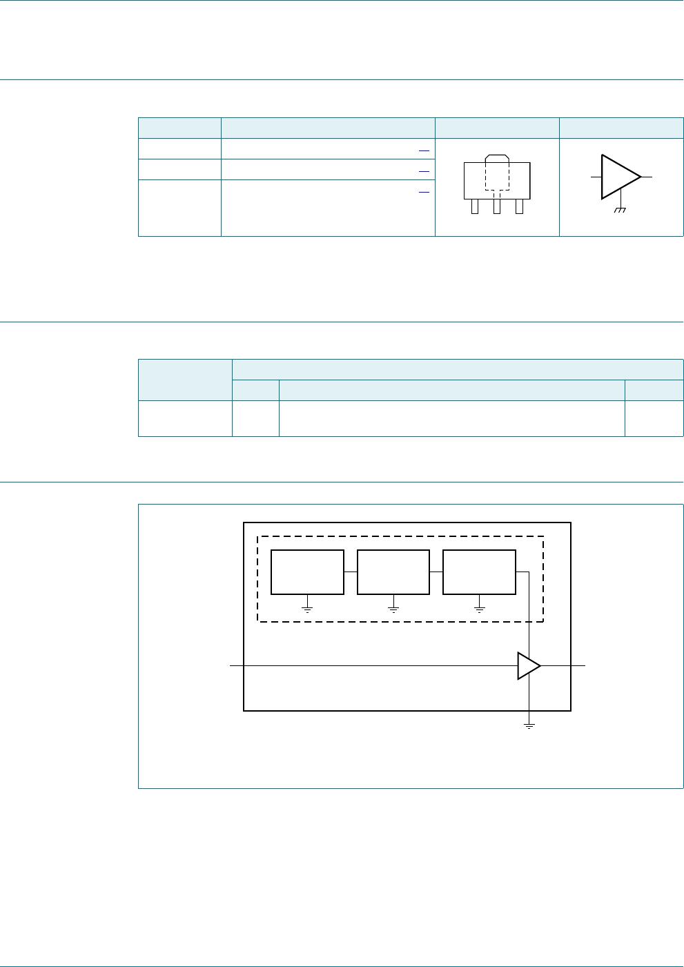
[1] Case is ground solder pad.
[2] Thermal resistance measured using infrared measurement technique, device mounted on application board
and placed in still air.
7. Static characteristics
8. Dynamic characteristics
Table 4. Limiting values
In accordance with the Absolute Maximum Rating System (IEC 60134).
Symbol Parameter Conditions Min Max Unit
V
CC(RF)
RF supply voltage - 5.7 V
P
i(RF)
RF input power - 25 dBm
T
case
case temperature 40 +85 C
T
j
junction temperature - 150 C
V
ESD
electrostatic discharge voltage Human Body Model (HBM);
according to JEDEC standard 22-A114E
-2000V
Charged Device Model (CDM);
according to JEDEC standard 22-C101B
-500V
Table 5. Thermal characteristics
Symbol Parameter Conditions Typ Unit
R
th(j-c)
thermal resistance from junction to case
[1][2]
25 K/W
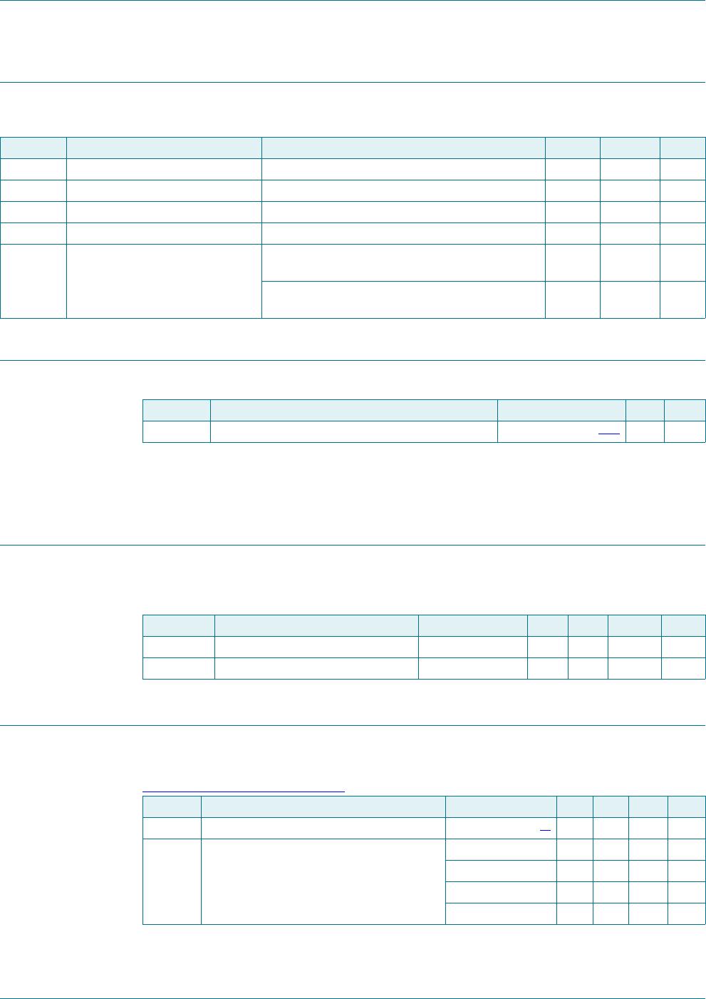
Table 6. Characteristics
Input and output impedances matched to 50
. Typical values at V
CC
=5V; T
case
=25
C; unless
otherwise specified.
Symbol Parameter Conditions Min Typ Max Unit
V
CC
supply voltage - 5.0 - V
I
CC
supply current 95 110 125 mA
Table 7. Dynamic characteristics
Input and output impedances matched to 50
. Typical values at V
CC
=5V; T
case
=25
C; see
Section 12 “
Application information; unless otherwise specified.
Symbol Parameter Conditions Min Typ Max Unit
f frequency
[1]
400 - 2700 MHz
G
p
power gain f = 940 MHz - 22 - dB
f = 1960 MHz - 16 - dB
f = 2140 MHz 13.5 15 16.5 dB
f = 2445 MHz - 14 - dB

BGA7024,135

Mfr. #:
Manufacturer:
NXP Semiconductors
Description:
RF Amplifier Driver Amplifier One-stage
Lifecycle:
New from this manufacturer.
Delivery:
DHL FedEx Ups TNT EMS
Payment:
T/T Paypal Visa MoneyGram Western Union

Products related to this Datasheet