BGA7024 All information provided in this document is subject to legal disclaimers. © NXP Semiconductors N.V. 2014. All rights reserved.
Product data sheet Rev. 3 — 11 June 2014 4 of 23
NXP Semiconductors
BGA7024
400 MHz to 2700 MHz 0.25 W high linearity silicon amplifier
[1] Operation outside this range is possible but not guaranteed.
[2] P
L
= 11 dBm per tone; spacing = 1 MHz.
[3] Defined at P
i(RF)
= 40 dBm; small signal conditions.
9. Scattering parameters
P
L(1dB)
output power at 1 dB gain compression f = 940 MHz - 24 - dBm
f = 1960 MHz - 25.5 - dBm
f = 2140 MHz 24.0 25.5 - dBm
f = 2445 MHz - 24.5 - dBm
IP3
O
output third-order intercept point f = 940 MHz
[2]
- 37.5 - dBm
f = 1960 MHz
[2]
- 38.0 - dBm
f = 2140 MHz
[2]
35.0 38.0 - dBm
f = 2445 MHz
[2]
- 37.5 - dBm
NF noise figure f = 940 MHz
[3]
-2.9- dB
f = 1960 MHz
[3]
-3.7- dB
f = 2140 MHz
[3]
-3.7- dB
f = 2445 MHz
[3]
-4.0- dB
RL
in
input return loss f = 940 MHz - 9- dB
f = 1960 MHz - 10 - dB
f = 2140 MHz - 10 - dB
f = 2445 MHz - 14 - dB
RL
out
output return loss f = 940 MHz - 29 - dB
f = 1960 MHz - 22 - dB
f = 2140 MHz - 29 - dB
f = 2445 MHz - 11 - dB
Table 7. Dynamic characteristics
…continued
Input and output impedances matched to 50
. Typical values at V
CC
=5V; T
case
=25
C; see
Section 12 “Application information”; unless otherwise specified.
Symbol Parameter Conditions Min Typ Max Unit
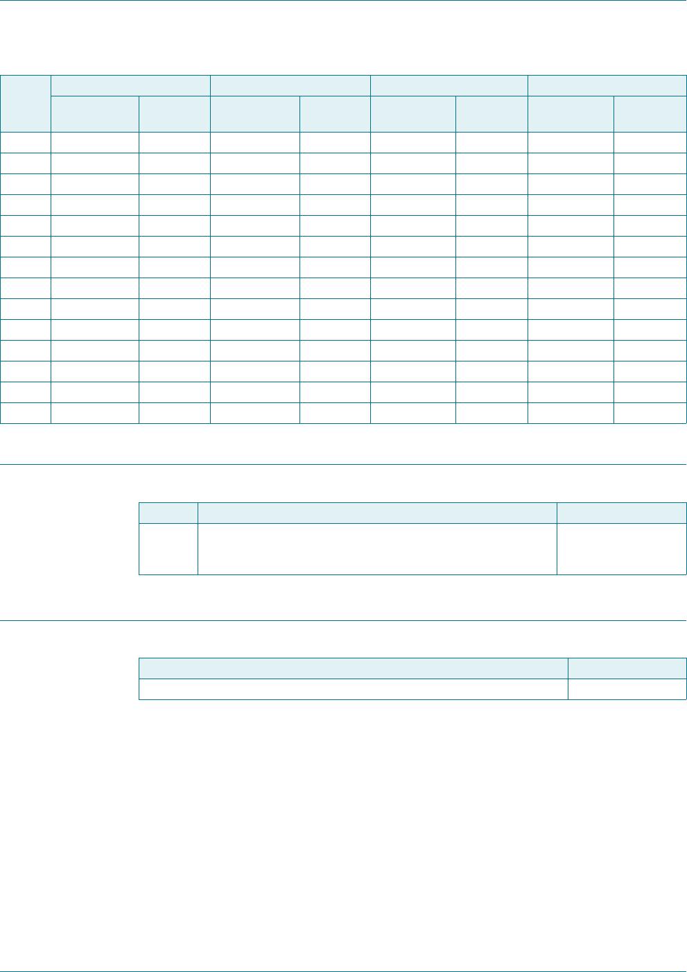
Table 8. Scattering parameters at 5 V, MMIC only
f (MHz) S
11
S
21
S
12
S
22
Magnitude
(ratio)
Angle
(degree)
Magnitude
(ratio)
Angle
(degree)
Magnitude
(ratio)
Angle
(degree)
Magnitude
(ratio)
Angle
(degree)
400 0.83 178.9 14.03 112.7 0.01 35.5 0.53 166.3
500 0.85 178.7 11.69 104.4 0.01 38.77 0.56 168.9
600 0.85 176.4 9.93 98.19 0.02 41.13 0.57 172.2
700 0.86 173.8 8.67 93.04 0.02 43.1 0.58 174.8
800 0.86 171.1 7.68 88.54 0.02 44.34 0.58 177.4
900 0.86 168.3 6.9 84.36 0.02 44.96 0.59 179.7
1000 0.86 165.4 6.29 80.24 0.02 45.07 0.60 176.7
1100 0.87 162.7 5.72 76.42 0.02 45 0.60 173.3
1200 0.88 159.9 5.23 72.83 0.02 44.54 0.60 170.9
1300 0.88 157.3 4.80 69.34 0.03 44.17 0.61 168.4