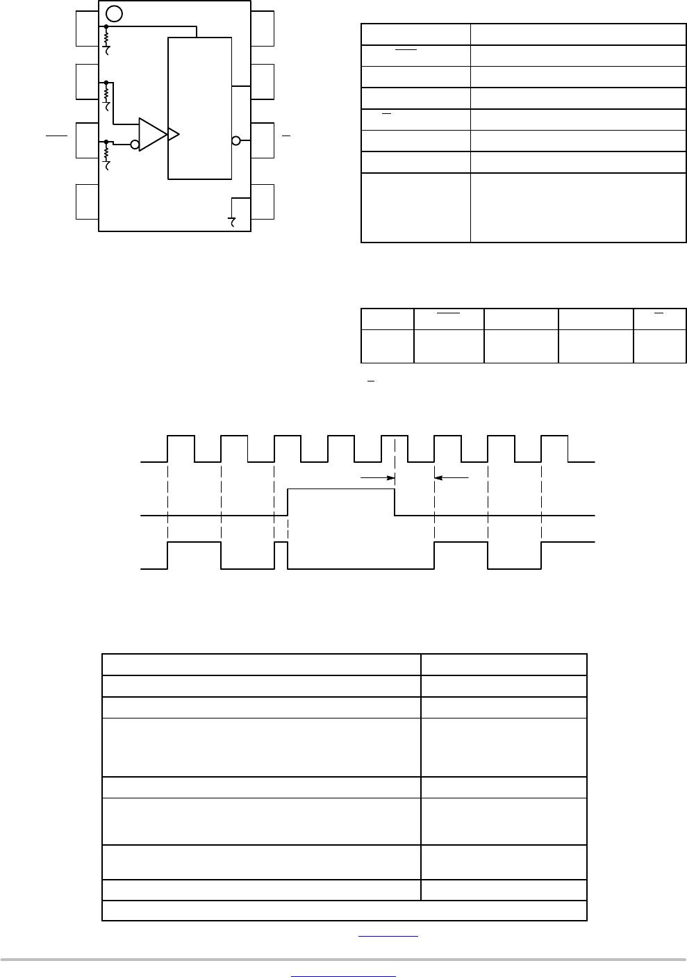
MC10EP32DTR2G

© Semiconductor Components Industries, LLC, 2016
July, 2016 Rev. 12
1 Publication Order Number:
MC10EP32/D
MC10EP32, MC100EP32
3.3V / 5V ECL B2 Divider
Description
The MC10/100EP32 is an integrated B2 divider with differential
CLK inputs.
The V
BB
pin, an internally generated voltage supply, is available to
this device only. For single-ended input conditions, the unused
differential input is connected to V
BB
as a switching reference voltage.
V
BB
may also rebias AC coupled inputs. When used, decouple V
BB
and V
CC
via a 0.01ĂmF capacitor and limit current sourcing or sinking
to 0.5 mA. When not used, V
BB
should be left open.
The reset pin is asynchronous and is asserted on the rising edge.
Upon power-up, the internal flip-flops will attain a random state; the
reset allows for the synchronization of multiple EP32’s in a system.
The 100 Series contains temperature compensation.
Features
350 ps Typical Propagation Delay
Maximum Frequency > 4 GHz Typical (Figure 3)
PECL Mode Operating Range:
V
CC
= 3.0 V to 5.5 V with V
EE
= 0 V
NECL Mode Operating Range:
V
CC
= 0 V with V
EE
= 3.0 V to 5.5 V
Open Input Default State
Safety Clamp on Inputs
Q Output Will Default LOW with Inputs Open or at V
EE
These Devices are Pb-Free, Halogen Free and are RoHS Compliant
A = Assembly Location
L = Wafer Lot
Y = Year
W = Work Week
G = Pb-Free Package
H = MC10
K = MC100
5P = MC10
3K = MC100
M
= Date Code
SOIC8NB
D SUFFIX
CASE
75107
MARKING DIAGRAMS*
TSSOP8
DT SUFFIX
CASE
948R02
ALYWG
G
HP32
ALYWG
G
KP32
1
8
1
8
1
8
www.onsemi.com
1
8
HEP32
ALYW
G
1
8
KEP32
ALYW
G
1
8
DFN8
MN SUFFIX
CASE 506AA
5P MG
G
14
3K MG
G
14
(Note: Microdot may be in either location)
*For additional marking information, refer to
Application Note AND8002/D
.
See detailed ordering and shipping information on page 8 of
this data sheet.
ORDERING INFORMATION
MC10EP32, MC100EP32
www.onsemi.com
2
1
2
3
45
6
7
8
Q
V
EE
V
CC
Figure 1. 8-Lead Pinout (Top View) and Logic
Diagram
CLK
Q
CLK
V
BB
RESET
R
B2
Table 1. PIN DESCRIPTION
Pin Function
CLK, CLK* ECL Clock Inputs
Reset* ECL Asynchronous Reset
V
BB
Reference Voltage Output
Q, Q ECL Data Outputs
V
CC
Positive Supply
V
EE
Negative Supply
EP (DFN8 only) Thermal exposed pad
must be connected to a sufficient thermal
conduit. Electrically connect to the most
negative supply (GND) or leave uncon-
nected, floating open.
*Pins will default LOW when left open.
Table 2. TRUTH TABLE
CLK CLK RESET Q Q
X
Z
X
Z
Z
L
L
F
H
F
Z = LOW to HIGH Transition
Z
= HIGH to LOW Transition
F = Divide by 2 Function
Figure 2. Timing Diagram
CLK
RESET
Q
t
RR
Table 3. ATTRIBUTES
Characteristics Value
Internal Input Pulldown Resistor
75 kW
Internal Input Pullup Resistor N/A
ESD Protection
Human Body Model
Machine Model
Charged Device Model
> 4 kV
> 200 V
> 2 kV
Moisture Sensitivity, Indefinite Time Out of Drypack (Note 1) Pb-Free Pkg
SOIC8NB
TSSOP8
DFN8
Level 1
Level 3
Level 1
Flammability Rating
Oxygen Index: 28 to 34
UL 94 V0 @ 0.125 in
Transistor Count 78 Devices
Meets or exceeds JEDEC Spec EIA/JESD78 IC Latchup Test
1. For additional information, see Application Note AND8003/D.
MC10EP32, MC100EP32
www.onsemi.com
3
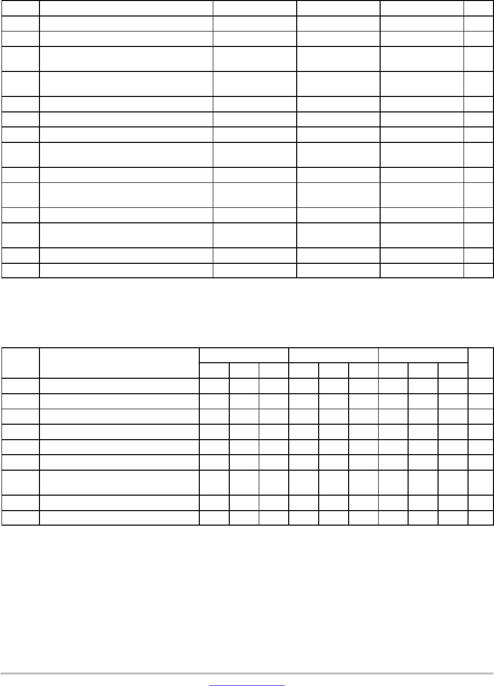
Table 4. MAXIMUM RATINGS
Symbol Parameter Condition 1 Condition 2 Rating Unit
V
CC
PECL Mode Power Supply V
EE
= 0 V 6 V
V
EE
NECL Mode Power Supply V
CC
= 0 V 6 V
V
I
PECL Mode Input Voltage
NECL Mode Input Voltage
V
EE
= 0 V
V
CC
= 0 V
V
I
v V
CC
V
I
w V
EE
6
6
V
I
out
Output Current Continuous
Surge
50
100
mA
I
BB
V
BB
Sink/Source ± 0.5 mA
T
A
Operating Temperature Range 40 to +85 °C
T
stg
Storage Temperature Range 65 to +150 °C
q
JA
Thermal Resistance (Junction-to-Ambient) 0 lfpm
500 lfpm
SOIC8NB 190
130
°C/W
q
JC
Thermal Resistance (Junction-to-Case) Standard Board SOIC8NB 41 to 44 °C/W
q
JA
Thermal Resistance (Junction-to-Ambient) 0 lfpm
500 lfpm
TSSOP8 185
140
°C/W
q
JC
Thermal Resistance (Junction-to-Case) Standard Board TSSOP8 41 to 44 °C/W
q
JA
Thermal Resistance (Junction-to-Ambient) 0 lfpm
500 lfpm
DFN8 129
84
°C/W
T
sol
Wave Solder (Pb-Free) <2 to 3 sec @ 260°C 265 °C
q
JC
Thermal Resistance (Junction-to-Case) (Note 1) DFN8 35 to 40 °C/W
Stresses exceeding those listed in the Maximum Ratings table may damage the device. If any of these limits are exceeded, device functionality
should not be assumed, damage may occur and reliability may be affected.
1. JEDEC standard multilayer board 2S2P (2 signal, 2 power)
Table 5. 10EP DC CHARACTERISTICS, PECL (V
CC
= 3.3 V, V
EE
= 0 V (Note 1))
Symbol
Characteristic
40°C 25°C 85°C
Unit
Min Typ Max Min Typ Max Min Typ Max
I
EE
Power Supply Current 23 30 40 23 30 40 23 30 40 mA
V
OH
Output HIGH Voltage (Note 2) 2165 2290 2415 2230 2355 2480 2290 2415 2540 mV
V
OL
Output LOW Voltage (Note 2) 1365 1490 1615 1430 1555 1680 1490 1615 1740 mV
V
IH
Input HIGH Voltage (Single-Ended) 2090 2415 2155 2480 2215 2540 mV
V
IL
Input LOW Voltage (Single-Ended) 1365 1690 1430 1755 1490 1815 mV
V
BB
Output Voltage Reference 1790 1890 1990 1855 1955 2055 1915 2015 2115 mV
V
IHCMR
Input HIGH Voltage Common Mode
Range (Differential Configuration) (Note 3)
2.0 3.3 2.0 3.3 2.0 3.3 V
I
IH
Input HIGH Current 150 150 150
mA
I
IL
Input LOW Current 0.5 0.5 0.5
mA
NOTE: Device will meet the specifications after thermal equilibrium has been established when mounted in a test socket or printed circuit
board with maintained transverse airflow greater than 500 lfpm. Electrical parameters are guaranteed only over the declared
operating temperature range. Functional operation of the device exceeding these conditions is not implied. Device specification limit
values are applied individually under normal operating conditions and not valid simultaneously.
1. Input and output parameters vary 1:1 with V
CC
. V
EE
can vary +0.3 V to 2.2 V.
2. All loading with 50 W to V
CC
2.0 V.
3. V
IHCMR
min varies 1:1 with V
EE
, V
IHCMR
max varies 1:1 with V
CC
. The V
IHCMR
range is referenced to the most positive side of the differential
input signal.

MC10EP32DTR2G

Mfr. #:
Manufacturer:
ON Semiconductor
Description:
Multipliers / Dividers 3.3V/5V ECL Divide By 2 Divider
Lifecycle:
New from this manufacturer.
Delivery:
DHL FedEx Ups TNT EMS
Payment:
T/T Paypal Visa MoneyGram Western Union