MC10EP32DTR2G

MC10EP32, MC100EP32
www.onsemi.com
4
Table 6. 10EP DC CHARACTERISTICS, PECL (V
CC
= 5.0 V, V
EE
= 0 V (Note 1))
Symbol
Characteristic
40°C 25°C 85°C
Unit
Min Typ Max Min Typ Max Min Typ Max
I
EE
Power Supply Current 23 30 40 23 30 40 23 30 40 mA
V
OH
Output HIGH Voltage (Note 2) 3865 3990 4115 3930 4055 4180 3990 4115 4240 mV
V
OL
Output LOW Voltage (Note 2) 3065 3190 3315 3130 3255 3380 3190 3315 3440 mV
V
IH
Input HIGH Voltage (Single-Ended) 3790 4115 3855 4180 3915 4240 mV
V
IL
Input LOW Voltage (Single-Ended) 3065 3390 3130 3455 3190 3515 mV
V
BB
Output Voltage Reference 3490 3590 3690 3555 3655 3755 3615 3715 3815 mV
V
IHCMR
Input HIGH Voltage Common Mode Range
(Differential Configuration) (Note 3)
2.0 5.0 2.0 5.0 2.0 5.0 V
I
IH
Input HIGH Current 150 150 150
mA
I
IL
Input LOW Current 0.5 0.5 0.5
mA
NOTE: Device will meet the specifications after thermal equilibrium has been established when mounted in a test socket or printed circuit
board with maintained transverse airflow greater than 500 lfpm. Electrical parameters are guaranteed only over the declared
operating temperature range. Functional operation of the device exceeding these conditions is not implied. Device specification limit
values are applied individually under normal operating conditions and not valid simultaneously.
1. Input and output parameters vary 1:1 with V
CC
. V
EE
can vary +2.0 V to 0.5 V.
2. All loading with 50 W to V
CC
2.0 V.
3. V
IHCMR
min varies 1:1 with V
EE
, V
IHCMR
max varies 1:1 with V
CC
. The V
IHCMR
range is referenced to the most positive side of the differential
input signal.
Table 7. 10EP DC CHARACTERISTICS, NECL (V
CC
= 0 V; V
EE
= 5.5 V to 3.0 V (Note 1))
Symbol Characteristic
40°C 25°C 85°C
Unit
Min Typ Max Min Typ Max Min Typ Max
I
EE
Power Supply Current 23 30 40 23 30 40 23 30 40 mA
V
OH
Output HIGH Voltage (Note 2) 1135 1010 885 1070 945 820 1010 885 760 mV
V
OL
Output LOW Voltage (Note 2) 1935 1810 1685 1870 1745 1620 1810 1685 1560 mV
V
IH
Input HIGH Voltage (Single-Ended) 1210 885 1145 820 1085 760 mV
V
IL
Input LOW Voltage (Single-Ended) 1935 1610 1870 1545 1810 1485 mV
V
BB
Output Voltage Reference 1510 1410 1310 1445 1345 1245 1385 1285 1185 mV
V
IHCMR
Input HIGH Voltage Common Mode
Range (Differential Configuration)
(Note 3)
V
EE
+2.0 0.0 V
EE
+2.0 0.0 V
EE
+2.0 0.0 V
I
IH
Input HIGH Current 150 150 150
mA
I
IL
Input LOW Current 0.5 0.5 0.5
mA
NOTE: Device will meet the specifications after thermal equilibrium has been established when mounted in a test socket or printed circuit
board with maintained transverse airflow greater than 500 lfpm. Electrical parameters are guaranteed only over the declared
operating temperature range. Functional operation of the device exceeding these conditions is not implied. Device specification limit
values are applied individually under normal operating conditions and not valid simultaneously.
1. Input and output parameters vary 1:1 with V
CC
.
2. All loading with 50 W to V
CC
2.0 V.
3. V
IHCMR
min varies 1:1 with V
EE
, V
IHCMR
max varies 1:1 with V
CC
. The V
IHCMR
range is referenced to the most positive side of the differential
input signal.
MC10EP32, MC100EP32
www.onsemi.com
5
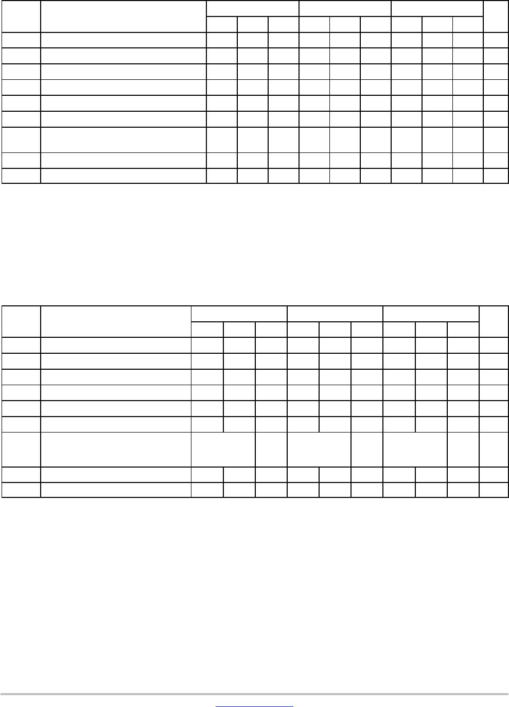
Table 8. 100EP DC CHARACTERISTICS, PECL (V
CC
= 3.3 V, V
EE
= 0 V (Note 1))
Symbol
Characteristic
40°C 25°C 85°C
Unit
Min Typ Max Min Typ Max Min Typ Max
I
EE
Power Supply Current 23 30 37 26 34 40 28 36 42 mA
V
OH
Output HIGH Voltage (Note 2) 2155 2280 2405 2155 2280 2405 2155 2280 2405 mV
V
OL
Output LOW Voltage (Note 2) 1355 1480 1605 1355 1480 1605 1355 1480 1605 mV
V
IH
Input HIGH Voltage (Single-Ended) 2075 2420 2075 2420 2075 2420 mV
V
IL
Input LOW Voltage (Single-Ended) 1355 1675 1355 1675 1355 1675 mV
V
BB
Output Voltage Reference 1775 1875 1975 1775 1875 1975 1775 1875 1975 mV
V
IHCMR
Input HIGH Voltage Common Mode Range
(Differential Configuration) (Note 3)
2.0 3.3 2.0 3.3 2.0 3.3 V
I
IH
Input HIGH Current 150 150 150
mA
I
IL
Input LOW Current 0.5 0.5 0.5
mA
NOTE: Device will meet the specifications after thermal equilibrium has been established when mounted in a test socket or printed circuit
board with maintained transverse airflow greater than 500 lfpm. Electrical parameters are guaranteed only over the declared
operating temperature range. Functional operation of the device exceeding these conditions is not implied. Device specification limit
values are applied individually under normal operating conditions and not valid simultaneously.
1. Input and output parameters vary 1:1 with V
CC
. V
EE
can vary +0.3 V to 2.2 V.
2. All loading with 50 W to V
CC
2.0 V.
3. V
IHCMR
min varies 1:1 with V
EE
, V
IHCMR
max varies 1:1 with V
CC
. The V
IHCMR
range is referenced to the most positive side of the differential
input signal.
Table 9. 100EP DC CHARACTERISTICS, PECL (V
CC
= 5.0 V, V
EE
= 0 V (Note 1))
Symbol Characteristic
40°C 25°C 85°C
Unit
Min Typ Max Min Typ Max Min Typ Max
I
EE
Power Supply Current 23 30 37 26 34 40 28 36 42 mA
V
OH
Output HIGH Voltage (Note 2) 3855 3980 4105 3855 3980 4105 3855 3980 4105 mV
V
OL
Output LOW Voltage (Note 2) 3055 3180 3305 3055 3180 3305 3055 3180 3305 mV
V
IH
Input HIGH Voltage (Single-Ended) 3775 4120 3775 4120 3775 4120 mV
V
IL
Input LOW Voltage (Single-Ended) 3055 3375 3055 3375 3055 3375 mV
V
BB
Output Voltage Reference 3475 3575 3675 3475 3575 3675 3475 3575 3675 mV
V
IHCMR
Input HIGH Voltage Common Mode Range
(Differential Configuration) (Note 3)
2.0 5.0 2.0 5.0 2.0 5.0 V
I
IH
Input HIGH Current 150 150 150
mA
I
IL
Input LOW Current 0.5 0.5 0.5
mA
NOTE: Device will meet the specifications after thermal equilibrium has been established when mounted in a test socket or printed circuit
board with maintained transverse airflow greater than 500 lfpm. Electrical parameters are guaranteed only over the declared
operating temperature range. Functional operation of the device exceeding these conditions is not implied. Device specification limit
values are applied individually under normal operating conditions and not valid simultaneously.
1. Input and output parameters vary 1:1 with V
CC
. V
EE
can vary +2.0 V to 0.5 V.
2. All loading with 50 W to V
CC
2.0 V.
3. V
IHCMR
min varies 1:1 with V
EE
, V
IHCMR
max varies 1:1 with V
CC
. The V
IHCMR
range is referenced to the most positive side of the differential
input signal.
MC10EP32, MC100EP32
www.onsemi.com
6
Table 10. 100EP DC CHARACTERISTICS, NECL (V
CC
= 0 V; V
EE
= 5.5 V to 3.0 V (Note 1))
Symbol
Characteristic
40°C 25°C 85°C
Unit
Min Typ Max Min Typ Max Min Typ Max
I
EE
Power Supply Current 23 30 37 26 34 40 28 36 42 mA
V
OH
Output HIGH Voltage (Note 2) 1145 1020 895 1145 1020 895 1145 1020 895 mV
V
OL
Output LOW Voltage (Note 2) 1945 1820 1695 1945 1820 1695 1945 1820 1695 mV
V
IH
Input HIGH Voltage (Single-Ended) 1225 880 1225 880 1225 880 mV
V
IL
Input LOW Voltage (Single-Ended) 1945 1625 1945 1625 1945 1625 mV
V
BB
Output Voltage Reference 1525 1425 1325 1525 1425 1325 1525 1425 1325 mV
V
IHCMR
Input HIGH Voltage Common Mode
Range (Differential Configuration)
(Note 3)
V
EE
+2.0 0.0 V
EE
+2.0 0.0 V
EE
+2.0 0.0 V
I
IH
Input HIGH Current 150 150 150
mA
I
IL
Input LOW Current 0.5 0.5 0.5
mA
NOTE: Device will meet the specifications after thermal equilibrium has been established when mounted in a test socket or printed circuit
board with maintained transverse airflow greater than 500 lfpm. Electrical parameters are guaranteed only over the declared
operating temperature range. Functional operation of the device exceeding these conditions is not implied. Device specification limit
values are applied individually under normal operating conditions and not valid simultaneously.
1. Input and output parameters vary 1:1 with V
CC
.
2. All loading with 50 W to V
CC
2.0 V.
3. V
IHCMR
min varies 1:1 with V
EE
, V
IHCMR
max varies 1:1 with V
CC
. The V
IHCMR
range is referenced to the most positive side of the differential
input signal.
Table 11. AC CHARACTERISTICS (V
CC
= 0 V; V
EE
= 3.0 V to 5.5 V or V
CC
= 3.0 V to 5.5 V; V
EE
= 0 V (Note 1))
Symbol
Characteristic
40°C 25°C 85°C
Unit
Min Typ Max Min Typ Max Min Typ Max
V
OPP
Output Voltage Amplitude (See Figure 3)
f
in
< 3.5 GHz
f
in
@ 4.0 GHz 640
700
740 630
700
710 500
700
600
mV
t
PLH
,
t
PHL
Propagation Delay to
Output Differential
CLK to Q, Q
10 Series
RESET to Q, Q
100 Series
RESET to Q, Q
250
220
320
330
290
400
420
390
480
270
250
320
350
300
400
450
390
480
320
320
375
400
380
450
480
460
525
ps
t
RR
Set/Reset Recovery 200 175 200 175 200 175 ps
t
PW
Minimum Pulse width
RESET
550 475 550 475 550 475 ps
t
JITTER
CLOCK Random Jitter (RMS)
f
in
< 3.5 GHz
f
in
@ v4.0 GHz
0.5
0.5 1.5
0.5
0.5 1.5
0.5
0.5 1.5
ps
V
PP
Input Voltage Swing
(Differential Configuration)
150 800 1200 150 800 1200 150 800 1200 mV
t
r
t
f
Output Rise/Fall Times
Q, Q
(20% 80%)
50 100 150 70 120 170 70 130 200 ps
NOTE: Device will meet the specifications after thermal equilibrium has been established when mounted in a test socket or printed circuit
board with maintained transverse airflow greater than 500 lfpm. Electrical parameters are guaranteed only over the declared
operating temperature range. Functional operation of the device exceeding these conditions is not implied. Device specification limit
values are applied individually under normal operating conditions and not valid simultaneously.
1. Measured using a 750 mV source, 50% duty cycle clock source. All loading with 50 W to V
CC
2.0 V.

MC10EP32DTR2G

Mfr. #:
Manufacturer:
ON Semiconductor
Description:
Multipliers / Dividers 3.3V/5V ECL Divide By 2 Divider
Lifecycle:
New from this manufacturer.
Delivery:
DHL FedEx Ups TNT EMS
Payment:
T/T Paypal Visa MoneyGram Western Union